IPC J-STD-003B.pdf - 第32页
5 EVALUATION AIDS 5.1 Evaluation Aids – Surface As an aid to evaluation of the test results (see Figure 5-1). This aid is to be used pri- marily to illustrate types of defects rather than percentage of area covered. 5.2 …
4.3.2 Test F1 – Wetting Balance Test: Lead-Free Sol-
der
This test is for wetting balance testing of plated-
through holes, surface conductors and attachment lands.
4.3.2.1 Apparatus A solder meniscus force measuring
device (wetting balance) which includes a temperature
controlled solder pot containing solder per 3.2.1 and main-
tained per 3.5.1 and 3.5.2 shall be used. The equipment
shall have a means of recording force as a function of time,
such as a chart recorder, data logger, or computer.
4.3.2.1.1 Dipping Device A mechanical or electrome-
chanical dipping device incorporated in the wetting balance
shall be used. The device shall be preset to produce an
immersion and emersion rate as specified in 4.3.1.3. The
test specimen dwell time is controlled to the time specified
in 4.3.1.3 (see Figure 4-7).
4.3.2.2 Test Specimen The test specimen shall be in
accordance with 1.7. The test specimen shall either be a
full board, a section of a board, or a suggested test speci-
men as illustrated in Figure 4-8. Test specimen preparation
shall be in accordance with 3.4.
4.3.2.3 Procedure After application of the flux and par-
tial drying per 4.1, the test specimen shall be mounted on
the test equipment. After blotting away excess flux from
the test specimen with a piece of absorbent clean material,
hang it on the apparatus so that its lower edge is 10 ± 1
mm [0.394 ± 0.039 in] above the solder bath to preheat it
for 20 ± 1 seconds. The test shall be started after clearing
of the surface dross from the molten solder and a waiting
period of5±5seconds for the bath to settle down.
The flux covered surface shall be immersed only once in
the molten solder to a depth of 0.20 ± 0.1 mm [0.00787 ±
0.0039 in]. The angle of immersion shall be 20 ° - 40 °. An
angle of 90 ° may be used only upon agreement between
user and vendor on immersion angle selection. The
immersion/emersion rate shall be1mm-5mm[0.039 in
- 0.20 in] per second and the dwell time shall be 5.0 +
0/-0.5 seconds. Prior to examination, all test specimens
shall have the flux removed using a cleaning agent in
accordance with 3.2.3 (see Figure 4-9).
4.3.2.4 Evaluation This test is intended for evaluation
purposes only (see 1.3).
4.3.2.4.1 Magnification Test specimens shall be exam-
ined at 10X using the equipment specified in 3.3.3.
4.3.2.4.2 Suggested Criteria The suggested criteria sets
for solderability evaluation are listed in Table 4-6. Figures
4-10 and 4-11 illustrate the suggested criteria of Table 4-6.
In addition, the area of the test sample with fresh solder
adhesion shall be greater than the area that was immersed
in the solder bath, (i.e., the printed board shall exhibit
positive solder wetting beyond its immersion depth).
4.3.2.5 Gauge Repeatability and Reproducibility (GR&R)
Protocol
Appendix D contains a suggested GR&R proto-
col that may be used by the vendor and user to insure that
the respective wetting balance equipment are correctly
calibrated.
Table 4-6 Wetting Balance Parameter and Suggested Criteria
Parameter Description
Suggested Criteriaa
Set A Set B
T
o
Time to buoyancy corrected zero ≤1 second ≤2 second
F2
Wetting force at two seconds from
start of test
≥50% of maximum theoretical
wetting force at or before two
secondsb
Positive value at or before two
seconds
F5
Wetting force at five seconds from
start of test
At or above the value of F2 At or above the value of F2
AA
Integrated value of area of the
wetting curve from start of test
≥ area calculated using sample
buoyancy and 50% maximum
theoretical forcec
> zero (0)
a. These suggested criteria have been established in a two-tier evaluation format with Set A being more stringent. Components meeting Set A suggested
criteria are applicable to a larger soldering process window than components meeting Set B suggested criteria. It should be recognized that components
meeting Set B suggested criteria may be completely acceptable to a larger process window but the user must determine which criteria set best integrates
into their process.
b. See Appendix A for the method of calculating the maximum theoretical force.
c. See Appendix B for the method of calculation. (It is suggested that this method of calculation be programmed into the software used for control of the wetting
balance test equipment.)
March 2007 IPC J-STD-003B
21
Copyright Association Connecting Electronics Industries
Provided by IHS under license with IPC
Not for Resale
No reproduction or networking permitted without license from IHS
--`,,```,,,,````-`-`,,`,,`,`,,`---
//^:^^#^~^^"^~"^"^:$^~#:"#:$@:~^"$^:#*~^$^~:^#*^^:^^*\\
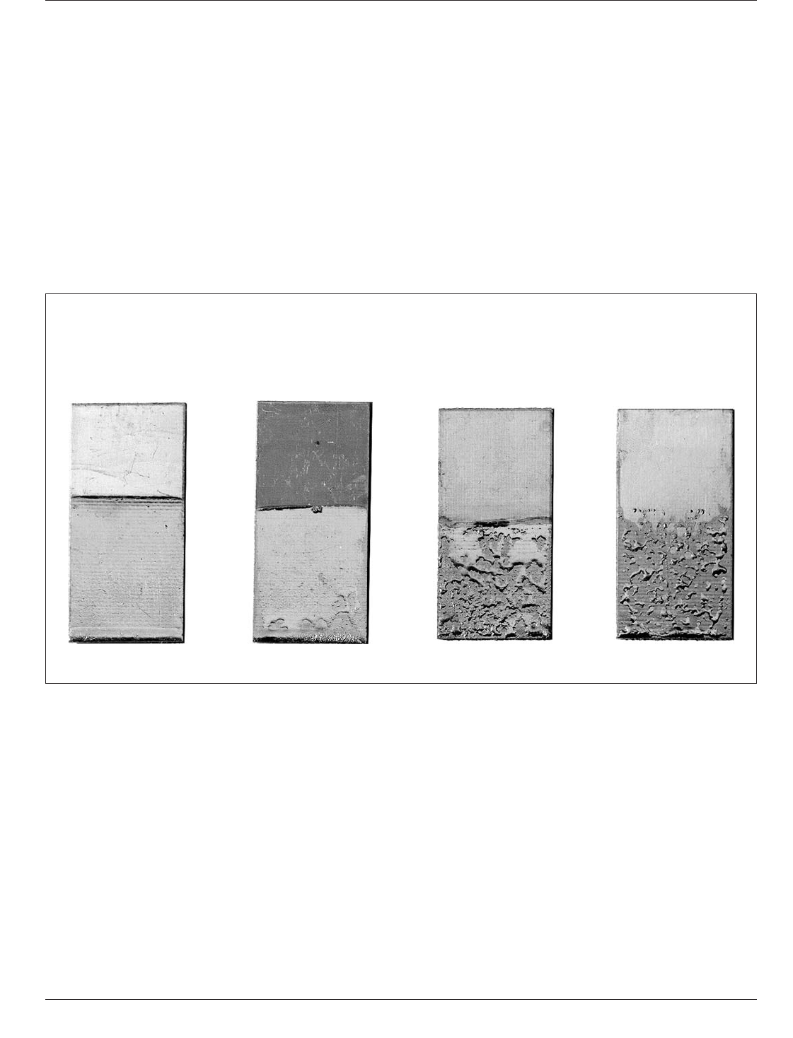
5 EVALUATION AIDS
5.1 Evaluation Aids – Surface
As an aid to evaluation of
the test results (see Figure 5-1). This aid is to be used pri-
marily to illustrate types of defects rather than percentage
of area covered.
5.2 Evaluation Aids – For Class 3 Plated-Through
Holes
Profile views of acceptable conditions are pre-
sented in Figure 4-5 for aid in visualizing all the common
conditions. The following are also acceptable conditions
for specific cases:
• Solderability acceptance for plated-through holes with
aspect ratios greater than 5:1 (board thickness: hole diam-
eter) shall be agreed upon by user and vendor.
• Depressed fillets in holes are acceptable under the follow-
ing condition: the solder in partially filled holes must
exhibit a contact angle less than 90 ° relative to the hole
wall (see Figure 4-5 and 4-6).
• All holes less than 1.5 mm [0.0591 in] diameter shall
retain a solder plug after solidification. Holes greater than
1.5 mm [0.0591 in] shall not be rejected for failure to
retain a full solder plug provided that the entire barrel of
the hole and the surface of the top land have been wetted
with solder (see Figures 4-5 and 4-6).
Preferred
Wetting
Small Amount
of Dewetting
Complete
Dewetting Nonwetting
IPC-003b-5-1
Figure 5-1 Aid to Evaluation
IPC J-STD-003B March 2007
22
Copyright Association Connecting Electronics Industries
Provided by IHS under license with IPC
Not for Resale
No reproduction or networking permitted without license from IHS
--`,,```,,,,````-`-`,,`,,`,`,,`---
//^:^^#^~^^"^~"^"^:$^~#:"#:$@:~^"$^:#*~^$^~:^#*^^:^^*\\

6 NOTES
6.1 Correction for Buoyancy
For the wetting balance to
obtain wetting force values that are comparable with one
another, it is necessary to correct for the variability in test
specimen sizes, particularly width and thickness. This is
done by correcting for the volume of the sample immersed
in the solder. The following formula may be used to calcu-
late the buoyant force correction:
F
b
= ρ gV
where:
ρ = Density of solder at 235 °C (8.12 g/cm) for Sn60/
Pb40 Alloy
ρ = Density of solder at 255 °C (7.41 g/cm) for SAC305
Alloy
g = Acceleration of gravity (981 cm/sec
2
)
V = Immersed volume of the test specimen (cm
3
)
= width x thickness x immersion depth, for example.
When the buoyancy force is calculated, it should be used
to correct the zero axis. This correction is required to
obtain both the proper measurement of wetting times, as
well as wetting forces. All measurements of wetting times
and wetting forces must be made from the corrected zero
axis. In the case of an upright curve, the new corrected zero
axis will be below the instrumental zero.
6.2 Preheat If the board test specimen does not pass the
standard solderability test then a uniform preheat of a sec-
ond test specimen may be used to determine if design/
construction has impacted the solderability test (i.e., a thick
board with heavy internal ground planes). If this referee
test specimen passes, then testing with preheat shall be the
method of choice for future testing of test specimens hav-
ing that design/construction.
6.3 Baking The occurrence of outgassing, which may
result in blowholes, measling, blisters or delamination, may
be reduced by baking the printed board prior to soldering
to eliminate moisture or solvents. Other factors, such as
conveyor speed (for wave solder testing), solder tempera-
ture, contamination content, etc., may also cause defects
and, therefore, should be analyzed if problems occur. Test
specimens should be baked in a suitable oven to remove
any absorbed moisture. Temperature and time of baking is
to be determined on an individual basis.
The time between baking and solderability testing should
be kept to a minimum (not more than 24 hours) in order to
prevent re-absorption of water vapor into the laminate
structure. The actual time delay threshold is dependent
upon ambient temperature and humidity levels.
6.4 Prebaking Printed boards should be prebaked only if
prebaking is normally used as a production procedure.
Baking should be kept to a minimum, adhering to the pro-
duction procedure, to prevent excessive oxidation and
intermetallic growth.
6.5 Safety Note Care must be taken in both usage and
storage to keep flammable solvents from sparks or flames.
See the Material Safety Data Sheets (MSDS) for all sol-
vents. All chemicals shall be handled per appropriate data
sheets, and disposed of per local regulations.
6.6 Use of Nonactivated Flux This standard specifies a
rosin-based flux with a very specific quantity of activator.
The intent of requiring the use of a specific quantity of flux
activator is to reduce the variability of test results that were
seen with pure rosin flux, enable the solderability testing of
nontin component lead metallizations, and provide a realis-
tic solderability testing safety factor by keeping the amount
of activator both fixed and less than that used for produc-
tion soldering. The benefit of using this specified activated
solderability testing flux composition was demonstrated by
extensive testing, as reported in the J-STD-002/003 Acti-
vated Solderability Test Flux Rationale Committee Letter.
6.7 Solder Contact The solder applied during the solder-
ability test must contact a feature in order for that feature
to be considered for evaluation. Small features surrounded
by a thick solder mask may prevent solder contact.
March 2007 IPC J-STD-003B
23
Copyright Association Connecting Electronics Industries
Provided by IHS under license with IPC
Not for Resale
No reproduction or networking permitted without license from IHS
--`,,```,,,,````-`-`,,`,,`,`,,`---
//^:^^#^~^^"^~"^"^:$^~#:"#:$@:~^"$^:#*~^$^~:^#*^^:^^*\\