IPC J-STD-003B.pdf - 第22页
process controls, incline, board preheat temperature and solder temperature. The application of solder shall meet the requirements of the applicable wave solder equipment, spe- cifically for depth of contact, angle of con…

enough to support the weight of the solder needed to fill the
hole. This may prevent solder from filling the plated-
through hole and wetting over the knee of the hole and out
onto the land area around the top of the hole.
4.2.3 Test C – Solder Float Test Tin/Lead Solder This
test is for solder float testing of plated-through holes, sur-
face conductors and attachment lands.
4.2.3.1 Apparatus
4.2.3.1.1 Solder Pot
The solder pot shall meet the
requirements of 3.3.2. In addition, the surface area of the
pot shall be great enough to float the test specimen without
it touching the sides of the pot.
4.2.3.1.2 Test Specimen Handling Tool Stainless steel
forceps, or other specially designed tools of stainless steel,
shall be used to handle the test specimen only by the
edges.
4.2.3.2 Test Specimen The test specimen shall be in
accordance with 1.7. The test specimen shall be a portion
of the printed board not greater than 50 x 50 mm [1.97 x
1.97 in], the suggested test specimen, or the complete
board if it is smaller than this size. The minimum number
of holes to be tested is 30 per test lot. If there are not at
least 30 holes in the test specimen, additional specimens
shall be tested until at least 30 holes have been tested (see
Figure 4-2 Through-Hole Test specimen). Test specimen
preparation shall be in accordance with 3.4.
4.2.3.3 Procedure Dross and burned/residual flux shall
be completely removed from the surface of the molten sol-
der immediately prior to floating. After fluxing and drain-
ing per 4.1, slide the test specimen gently on the molten
solder. Allow test specimen to float on solder for five sec-
onds maximum. The test specimen may be depressed into
the solder bath to a maximum of 50% of the test specimen
thickness after it has been initially floated on the solder
bath (extreme care must be taken with boards that are less
than 0.8 mm [0.031 in] thick). After the elapsed time, slide
the test specimen off molten solder. Hold test specimen still
and horizontal until solder solidifies. Prior to examination,
all test specimens shall have the flux removed using a
cleaning agent in accordance with 3.2.3.
4.2.3.4 Evaluation
4.2.3.4.1 Magnification
Test specimens shall be exam-
ined at 10X using the equipment specified in 3.3.3.
4.2.3.4.2 Surface Evaluation – Accept/Reject Criteria
An area of 3.0 mm [0.118 in] width from the trailing edge
of each test specimen shall not be evaluated. Areas con-
tacted by fixtures shall not be evaluated. A minimum of
95% of each of the surfaces (i.e., each pad) being tested
shall exhibit good wetting. The balance of the surface may
contain only small pin holes, dewetted areas, and rough
spots provided such defects are not concentrated in one
area. For less critical applications, a smaller percent cover-
age may be determined between vendor and user. There
shall be no nonwetting or exposed base metal within the
evaluated area.
4.2.3.4.3 Plated-Through Hole Evaluation Only plated-
through holes that are at least 3.0 mm [0.118 in] from any
surface or fixturing structure supporting the test specimen
during the test will be evaluated.
Accept/Reject Criteria:
• Class 1 and 2 Product – Solder shall fully wet the wall
area of the plated-through holes, and plug holes less than
1.5 mm [0.0591 in] diameter (complete filling is not nec-
essary).
• Class 3 Product – The test specimen has soldered suc-
cessfully if solder has risen in all plated-through holes.
The solder shall have fully wetted the walls of the hole.
There shall be no nonwetting or exposed base metal on
any plated-through hole.
Accept/reject criterion for board thicknesses of <3.0 mm
[<0.118 in] shall be in accordance with 5.2 and Figures 4-5
and 4-6. The solder must have wet over the knee of the
hole and out onto the land around the top of the hole,
except for boards whose thickness exceeds 3.0 mm [0.118
in].
On thick boards, i.e., greater than 3.0 mm [0.118 in] the
capillary forces due to surface tension may not be large
enough to support the weight of the solder needed to fill the
hole. This may prevent solder from filling the plated-
through hole and wetting over the knee of the hole and out
onto the land area around the top of the hole.
4.2.4 Test D – Wave Solder Test Tin/Lead Solder This
test is for wave solder testing of plated-through holes, sur-
face conductors, and attachment lands.
4.2.4.1 Apparatus A wave soldering system adjusted to
provide the parameters of 4.2.4.3 shall be used.
4.2.4.2 Test Specimen The suggested test specimen
shall be in accordance with Figures 4-2 and 4-3 and 1.7.
Test specimen preparation shall be in accordance with 3.4.
4.2.4.3 Procedure Test specimens shall be fixtured so as
to be representative of the production setup without com-
ponents inserted. The fluxing unit should be filled with the
specific (3.2.2) or agreed upon flux. If the unit contains
other than the specified or agreed upon flux then the flux-
ing unit shall be turned off and the board test specimens
fluxed separately prior to placement on the conveyor per
4.1. The following parameters must be established and
noted: board fixturing (if required), conveyor speed, pre-
heater, solder unit with or without oil intermix, machine
March 2007 IPC J-STD-003B
11
Copyright Association Connecting Electronics Industries
Provided by IHS under license with IPC
Not for Resale
No reproduction or networking permitted without license from IHS
--`,,```,,,,````-`-`,,`,,`,`,,`---
//^:^^#^~^^"^~"^"^:$^~#:"#:$@:~^"$^:#*~^$^~:^#*^^:^^*\\
process controls, incline, board preheat temperature and
solder temperature. The application of solder shall meet the
requirements of the applicable wave solder equipment, spe-
cifically for depth of contact, angle of contact, and duration
of contact. Solder temperature shall be235±5°C[455 ±
9 °F] unless another temperature is agreed upon by vendor
and user. Prior to examination, all test specimens shall
have the flux removed using a cleaning agent in accordance
with 3.2.3.
4.2.4.4 Evaluation
4.2.4.4.1 Magnification
Test specimens shall be exam-
ined at 10X using the equipment specified in 3.3.3.
4.2.4.4.2 Surface Evaluation – Accept/Reject Criteria
An area of 3.0 mm [0.118 in] width from the trailing edge
of each test specimen shall not be evaluated. Areas con-
tacted by fixtures shall not be evaluated. A minimum of
95% of each of the surfaces (i.e., each pad) being tested
shall exhibit good wetting. The balance of the surface may
contain only small pin holes, dewetted areas, and rough
spots provided such defects are not concentrated in one
area. For less critical applications, a smaller percent cover-
age may be determined between vendor and user. There
shall be no nonwetting or exposed base metal within the
evaluated area.
4.2.4.4.3 Plated-Through Hole Evaluation Only plated-
through holes that are at least 5.0 mm [0.197 in] from any
surface or fixturing structure supporting the test specimen
during the test will be evaluated.
Accept/Reject Criteria:
• Class 1 and 2 Product – Solder shall fully wet the wall
area of the plated-through holes, and plug holes less than
1.5 mm [0.0591 in] diameter (complete filling is not nec-
essary).
• Class 3 Product – The test specimen has soldered suc-
cessfully if solder has risen in all plated-through holes.
The solder shall have fully wetted the walls of the hole.
There shall be no nonwetting or exposed base metal on
any plated-through hole.
Accept/reject criteria for board thicknesses of <3.0 mm
[<0.118 in] shall be in accordance with 5.2 and Figures 4-5
and 4-6. The solder must have wetted over the knee of the
hole and out onto the land around the top of the hole,
except for boards whose thickness exceeds 3.0 mm [0.118
in].
On thick boards, i.e., greater than 3.0 mm [0.118 in], the
capillary action forces may not be large enough to over-
come forces exerted on the solder by the weight of the sol-
der. This may prevent solder from filling the plated-through
hole and wetting over the knee of the hole and out onto the
land area around the top of the hole.
4.2.5 Test E – Surface Mount Process Simulation Test
Tin/Lead Solder
This test simulates actual surface mount
printed board performance in a reflow process.
4.2.5.1 Apparatus
4.2.5.1.1 Stencil/Screen
A stencil or screen with pad
geometry openings that are appropriate for the test speci-
men shall be used. Unless otherwise agreed upon between
vendor and user the nominal stencil thickness shall be per
Table 4-1.
4.2.5.1.2 Paste Application Tool A rubber or metal
squeegee device shall be used to distribute paste across the
stencil/screen.
4.2.5.2 Test Specimen The test specimen shall be in
accordance with 1.7. The test specimen shall be tested in
the condition that it would normally experience at the time
of assembly soldering. The test specimen surfaces to be
tested shall be handled in such a manner as not to cause
contamination, nor shall the surfaces being tested be
wiped, cleaned, scraped or abraded.
4.2.5.3 Reflow Equipment An IR/convection reflow
oven, vapor phase reflow system, or storage oven capable
of reaching the reflow temperature of the paste shall
beused. The temperatures listed in Table 4-2 correspond to
the temperature/time duration for the solder paste. Addi-
tional time may be required to allow the test specimen
itself to reach the temperatures listed in Table 4-2. Unless
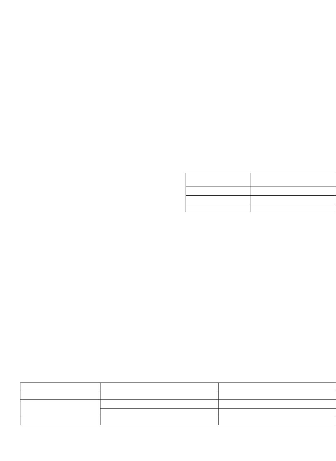
Table 4-2 Reflow Parameter Requirements
Reflow Type Temperature Time
Vapor Phase Reflow 215-219 °C [419-426 °F] 30-60 seconds dwell at reflow
IR/Convection Reflow
Preheat 150-170 °C [302-338 °F] 50-70 seconds
Reflow 215-230 °C [419-446 °F] 50-70 seconds
Oven 215-230 °C [419-446 °F] 2-5 minutes (until reflow is assured)
Table 4-1 Stencil Thickness Requirements
Nominal
Stencil Thickness Pitch
0.10 mm [0.00394 in] <0.50 mm [<0.0197 in]
0.15 mm [0.00591 in] 0.50-0.65 mm [0.0197-0.0256 in]
0.20 mm [0.00787 in] >0.65 mm [>0.0256 in]
IPC J-STD-003B March 2007
12
Copyright Association Connecting Electronics Industries
Provided by IHS under license with IPC
Not for Resale
No reproduction or networking permitted without license from IHS
--`,,```,,,,````-`-`,,`,,`,`,,`---
//^:^^#^~^^"^~"^"^:$^~#:"#:$@:~^"$^:#*~^$^~:^#*^^:^^*\\

otherwise agreed upon between vendor and user the reflow
parameters shall be per Table 4-2.
4.2.5.4 Procedure Place the stencil/screen on a surface
termination area of interest, apply solder paste (see 3.2.1)
onto the stencil/screen and print the stencil pattern onto the
test substrate by wiping paste over the stencil/screen in one
smooth motion using a rubber or metal squeegee. Remove
the stencil/screen carefully so as to avoid smearing the
paste print. Place test substrate on applicable reflow equip-
ment and conduct reflow process. After reflow, carefully
remove test specimen and allow to cool to room tempera-
ture. Prior to examination, all test specimens shall have the
flux removed using a cleaning agent in accordance with
3.2.3.
4.2.5.5 Evaluation
4.2.5.5.1 Magnification
Test specimens shall be exam-
ined at 10X using the equipment specified in 3.3.3.
4.2.5.5.2 Surface Evaluation – Accept/Reject Criteria
A minimum of 95% of each of the surfaces (i.e., each pad)
being tested shall exhibit good wetting. The balance of the
surface may contain only small pin holes, dewetted areas,
and rough spots provided such defects are not concentrated
in one area. For less critical applications, a smaller percent
coverage may be determined between vendor and user.
There shall be no nonwetting or exposed base metal within
the evaluated area.
March 2007 IPC J-STD-003B
13
Copyright Association Connecting Electronics Industries
Provided by IHS under license with IPC
Not for Resale
No reproduction or networking permitted without license from IHS
--`,,```,,,,````-`-`,,`,,`,`,,`---
//^:^^#^~^^"^~"^"^:$^~#:"#:$@:~^"$^:#*~^$^~:^#*^^:^^*\\