IPC J-STD-003B.pdf - 第19页
0.08 in]. The dwell time in the molten solder shall be 3.0 ± 0.5 seconds. Immersion and emersion rates shall be 25 ± 2 mm [0.984 ± 0.08 in] per second. After withdrawal, the solder shall be allowed to solidify by air coo…
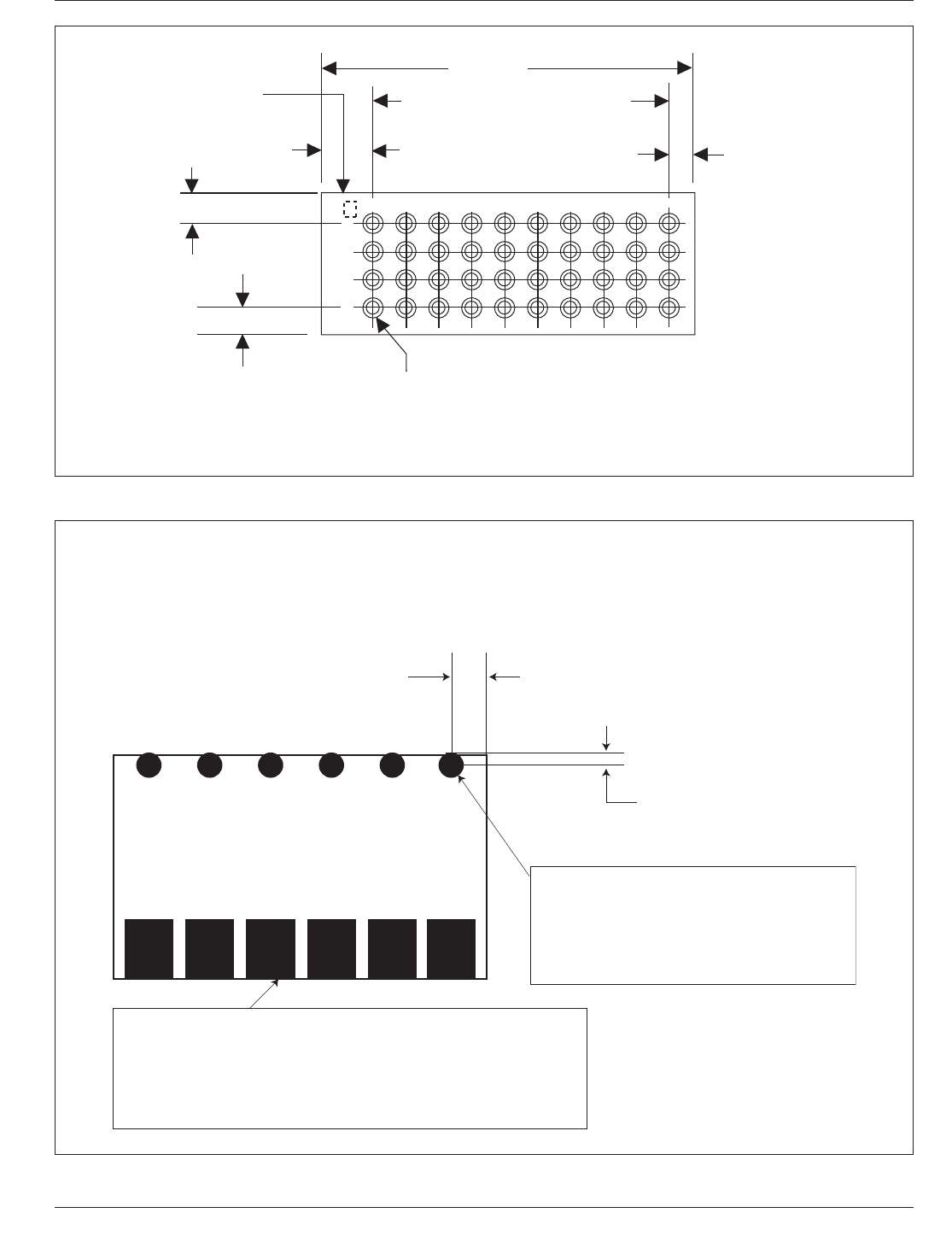
27.5 mm
[1.081 in]
2.0 mm
[0.0787 in]
22.5 mm
[0.8858 in]
7.5 mm [0.295 in]
2.5 mm [0.0984 in]
2.5 mm [0.0984 in]
Land Size 1.5 mm [0.0591 in]
40 Plated Through-Holes
0.8 ± 0.0125 mm [0.031 ± 0.0004921 in]
3.0 mm
[0.118 in]
2.5 mm
[0.0984 in]
9 Spaces @
S
Layer 1 Only
Appropriate
Specimen
Number
IPC-003b-4-2
Figure 4-2 Suggested Test Specimen for Plated-Through Holes
COMPONENT SIDE VIEW
Test Coupon size = 25 mm x 15 mm [0.984 in x 0.591 in]
SMD Pad Size = 3.18 mm x 4.52 mm [0.1250 in x 0.1780 in]
Pads are extended 0.51 mm [0.020 in] beyond the edge
Pad to pad pitch = 4.0 mm [0.157 in]
Mask clearance = 3.58 mm x 4.94 mm [0.1410 in x 0.1945 in]
Both sides
2.54 mm [0.1000 in]
0.94 mm [0.0370 in]
Pad Size (dia.) = 1.9 mm [0.0748 in]
Pad to pad pitch = 4.0 mm [0.157 in]
PTH size = 1.15 mm [0.0453 in] finished
Mask clearance = 2.31 mm [0.0909 in]
Both sides
IPC-003b-4-3
Figure 4-3 Suggested Test Specimen for Surface Mount Features
IPC J-STD-003B March 2007
8
Copyright Association Connecting Electronics Industries
Provided by IHS under license with IPC
Not for Resale
No reproduction or networking permitted without license from IHS
--`,,```,,,,````-`-`,,`,,`,`,,`---
//^:^^#^~^^"^~"^"^:$^~#:"#:$@:~^"$^:#*~^$^~:^#*^^:^^*\\
0.08 in]. The dwell time in the molten solder shall be 3.0
± 0.5 seconds. Immersion and emersion rates shall be 25 ±
2 mm [0.984 ± 0.08 in] per second. After withdrawal, the
solder shall be allowed to solidify by air cooling while the
board is maintained in a vertical position. Prior to exami-
nation, all test specimens shall have the flux removed using
a cleaning agent in accordance with 3.2.3.
4.2.1.4 Evaluation
4.2.1.4.1 Magnification
Test specimens shall be exam-
ined at 10X using the equipment specified in 3.3.3.
4.2.1.4.2 Surface Evaluation – Accept/Reject Criteria
A minimum of 95% of each of the surfaces (i.e., each pad)
being tested shall exhibit good wetting. The balance of the
surface may contain only small pin holes, dewetted areas,
and rough spots provided such defects are not concentrated
in one area. For less critical applications, a smaller percent
coverage may be determined between vendor and user.
There shall be no nonwetting or exposed base metal within
the evaluated area. An area of 3.2 mm [0.126 in] width
from the bottom edge of each test specimen shall not
be evaluated. Areas contacted by fixtures shall not be
evaluated.
4.2.2 Test B – Rotary Dip Test Tin/Lead Solder This
test is for rotary dip testing of plated-through holes, surface
conductors and attachment lands.
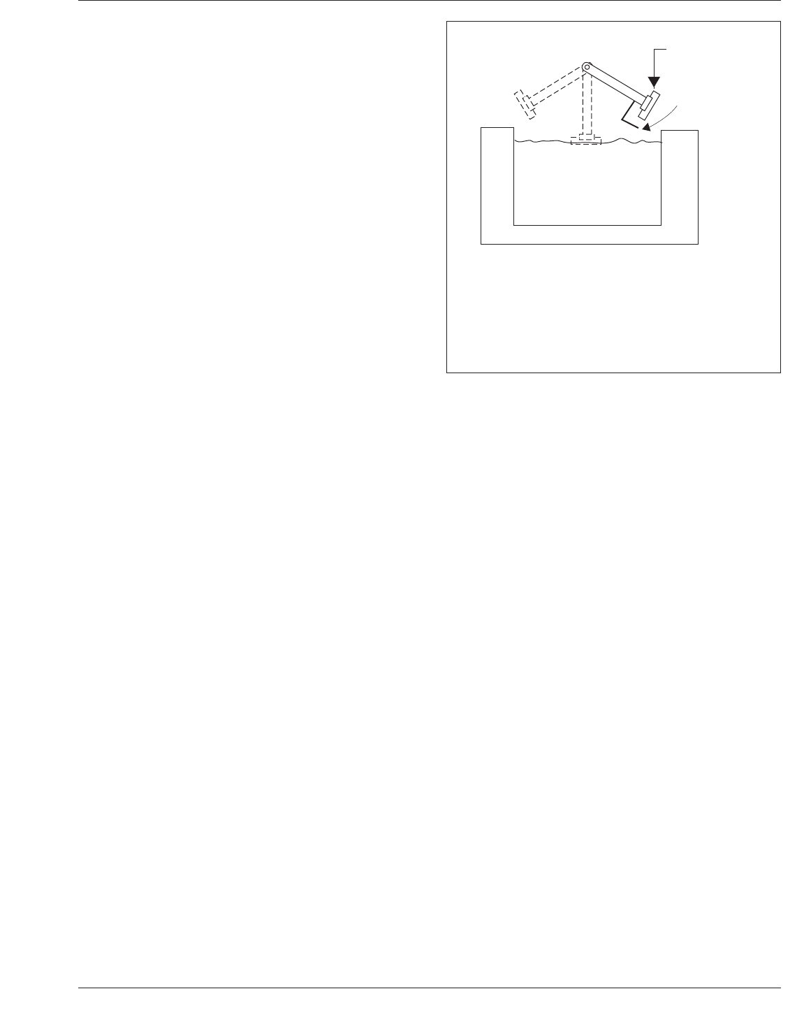
4.2.2.1 Apparatus A device shall be used to move the
test specimen in a circular path so that the flat surface of
the test specimen will contact the solder at a constant speed
without stopping. The distance between the center of rota-
tion and the center of the test specimen shall be 100 mm
[3.937 in] minimum. An example of a test specimen holder
is shown in Figure 4-4. Those parts of the holder including
the retaining spring (if fitted) which come into contact with
the test specimen and/or the solder should have low ther-
mal capacity and conductivity. The time of contact between
any point of the test face of the test specimen and the mol-
ten solder shall be determined by a timer. The timer shall
start when the face of the test piece is parallel to the solder
surface. A strip of 50 mm [1.97 in] wide polytetrafluoroet-
hylene (PTFE) or equivalent shall precede the test speci-
men in the test cycle in order to remove oxide or flux resi-
due from the solder surface immediately before the test
specimen is introduced.
4.2.2.2 Test Specimen The test specimen shall be in
accordance with 1.7. The test specimen shall either be a
full board, a section of a board, or a suggested test speci-
men (see Figures 4-2 and 4-3). The test specimen shall be
of such a width as to allow 13 mm [0.512 in] clearance
from the solder pot sides. The minimum number of termi-
nations (plated-through holes or attachment lands) per test
specimen shall be six. If plated-through holes are to be
tested, then the minimum number of holes to be tested is
30 per test lot. This would require a minimum of five test
specimens (six holes per test specimen, 30 holes total). The
test specimen shall be representative of the product. The
exposed length of test specimen test face in the direction of
travel shall be25±5mm[0.984 ± 0.20 in]. Test specimen
preparation shall be in accordance with 3.4.
4.2.2.3 Procedure Dross and burned/residual flux shall
be completely removed from the surface of the molten sol-
der immediately prior to dipping. After fluxing and drain-
ing, per 4.1, mount the test specimen to be tested in the test
equipment test specimen holder. Adjust the test equipment
to immerse the test specimen into the solder bath to a
maximum of 50% of the test specimen thickness unless
otherwise specified. Activate the test equipment to expose
the test specimen to solder. After the test specimen has
cleared the solder bath, allow all the solder to solidify in
the position in which the machine stops before removing
from the test specimen holder. Care must be taken so
that solder does not flow over the upper face of the test
specimen. This may be impacted by the width of the test
specimen. Dwell time at the maximum depth shall be 3.0
± 0.5 seconds. Prior to examination, all test specimens
shall have the flux removed using a cleaning agent in
accordance with 3.2.3.
4.2.2.4 Evaluation
4.2.2.4.1 Magnification
Test specimens shall be exam-
ined at 10X using the equipment specified in 3.3.3.
1) Dwell timer set at 3.0 ± 0.5 seconds
2) Adjustable speed control on 100.0 mm
[3.9370 in] radius on solder station
3) Dwell at end of 100.0 mm [3.9370 in]
radius swing to allow solder to solidify
Solder
Coupon
Dross
Wiper
IPC-003b-4-4
Figure 4-4 Rotary Dip Test
March 2007 IPC J-STD-003B
9
Copyright Association Connecting Electronics Industries
Provided by IHS under license with IPC
Not for Resale
No reproduction or networking permitted without license from IHS
--`,,```,,,,````-`-`,,`,,`,`,,`---
//^:^^#^~^^"^~"^"^:$^~#:"#:$@:~^"$^:#*~^$^~:^#*^^:^^*\\
4.2.2.4.2 Surface Evaluation – Accept/Reject Criteria
An area of 3.0 mm [0.118 in] width from the trailing edge
of each test specimen shall not be evaluated. Areas con-
tacted by fixtures shall not be evaluated. A minimum of
95% of each of the surfaces (i.e., each pad) being tested
shall exhibit good wetting. The balance of the surface may
contain only small pin holes, dewetted areas, and rough
spots provided such defects are not concentrated in one
area. For less critical applications, a smaller percent cover-
age may be determined between vendor and user. There-
shall be no nonwetting or exposed base metal within the
evaluated area.
4.2.2.4.3 Plated-Through Hole Evaluation Only plated-
through holes that are at least 5.0 mm [0.197 in] from any
surface or fixturing structure supporting the test specimen
during the test will be evaluated. An area of 3.0 mm [0.118
in] width from the trailing edge of each test specimen shall
not be evaluated. Areas contacted by fixtures shall not be
evaluated.
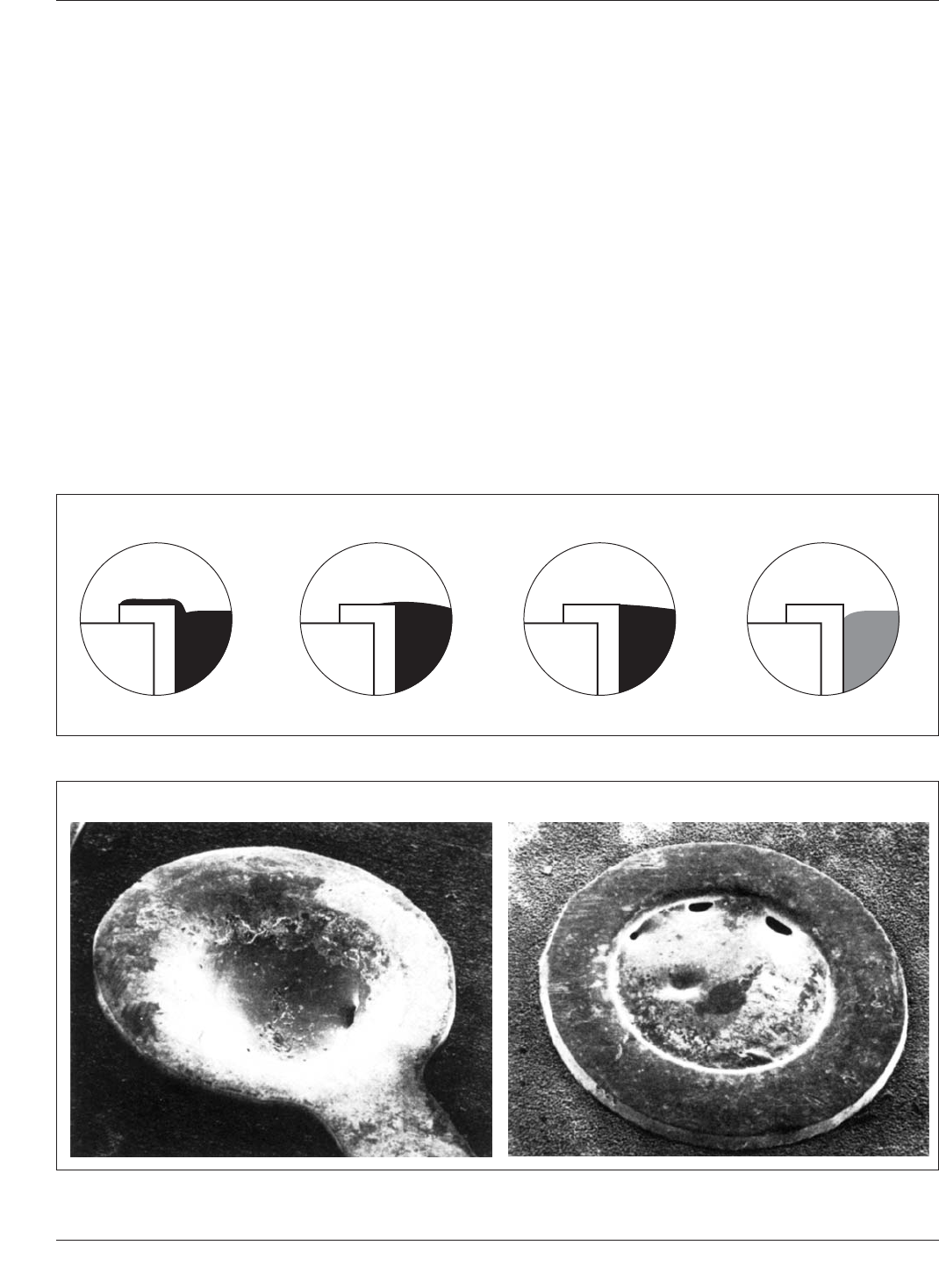
Accept/Reject Criteria:
• Class 1 and 2 Product – Solder shall fully wet the wall
area of the plated-through holes, and plug holes less than
1.5 mm [0.0591 in] diameter (complete filling is not
necessary).
• Class 3 Product – The test specimen has soldered
successfully if solder has risen in all plated-through holes.
The solder shall have fully wetted the walls of the hole.
There shall be no nonwetting or exposed base metal on
any plated-through hole.
Accept/reject criteria for boards thickness <3.0 mm
[<0.118 in] shall be in accordance with 5.2 and Figures 4-5
and 4-6. The solder must have wet over the knee of the
hole and out onto the land around the top of the hole,
except for boards whose thickness exceeds 3.0 mm [0.118
in].
On thick boards, i.e., greater than 3.0 mm [0.118 in] the
capillary forces due to surface tension may not be large
Target Condition
M
a
g
n
i
f
i
e
d
V
i
e
w
Acceptable Condition
M
a
g
n
i
f
i
e
d
V
i
e
w
Acceptable Condition
(for PCBs > 3.0 mm thk)
M
a
g
n
i
f
i
e
d
V
i
e
w
Nonacceptable Condition
M
a
g
n
i
f
i
e
d
V
i
e
w
IPC-003b-4-5
Figure 4-5 Effectiveness of Solder Wetting of Plated-Through Holes - Class 3
Figure 4-6 Examples of Solder Wetting of Plated-Through Holes - Class 3
Acceptable Condition Nonacceptable Condition
IPC J-STD-003B March 2007
10
Copyright Association Connecting Electronics Industries
Provided by IHS under license with IPC
Not for Resale
No reproduction or networking permitted without license from IHS
--`,,```,,,,````-`-`,,`,,`,`,,`---
//^:^^#^~^^"^~"^"^:$^~#:"#:$@:~^"$^:#*~^$^~:^#*^^:^^*\\