Specification SIPLACE X-Series S 规格说明书.pdf - 第38页
38 SIPLACE Vision OnBoard Inspection and Pattern Matching OnBoard Inspection The OnBoard PCB Inspec- tion (SW option) uses the PCB camera to inspect criti- cal areas of the board, spec- ified by the user, e.g. under BGA …

37
Component feeding
SIPLACE JTF-M
Technical data
SIPLACE JTF-M
Width
177 mm
Height
587 mm
JEDEC waffle pack tray specification
JEDEC Standard: 95-1 & IEC 60286-5
Storage capacity
Waffle pack tray, thin 18 JEDEC waffle pack trays
Thick waffle pack tray 14 JEDEC waffle pack trays
Waffle pack tray changeover time
Slot n to n+1 3.5 seconds
Slot 1 to 18 10 seconds
Slot 18 to 1 8.9 seconds
Cassette
Dimensions Approx. 330 mm x 150 mm x 230 mm
Max. load capacity 2.7 kg (150 g each for 18 slots)
Pneumatics
5.2 bar to 9 bar
Compressed air consumption
< 28.3 NL/min.
38
SIPLACE Vision
OnBoard Inspection and Pattern Matching
OnBoard Inspection
The OnBoard PCB Inspec-
tion (SW option) uses the
PCB camera to inspect criti-
cal areas of the board, spec-
ified by the user, e.g. under
BGA or shields just before or
after placement, to make
sure that all components
were placed or to make sure
that there are no objects in
the way of the placement
process.
It is also possible to inspect
the solder paste to make
sure that it is present. How-
ever, this must always be
performed at the first place-
ment machine, before any
placement begins.
A requirement for all inspec-
tion tasks is that a "good pat-
tern" has been saved before
starting.
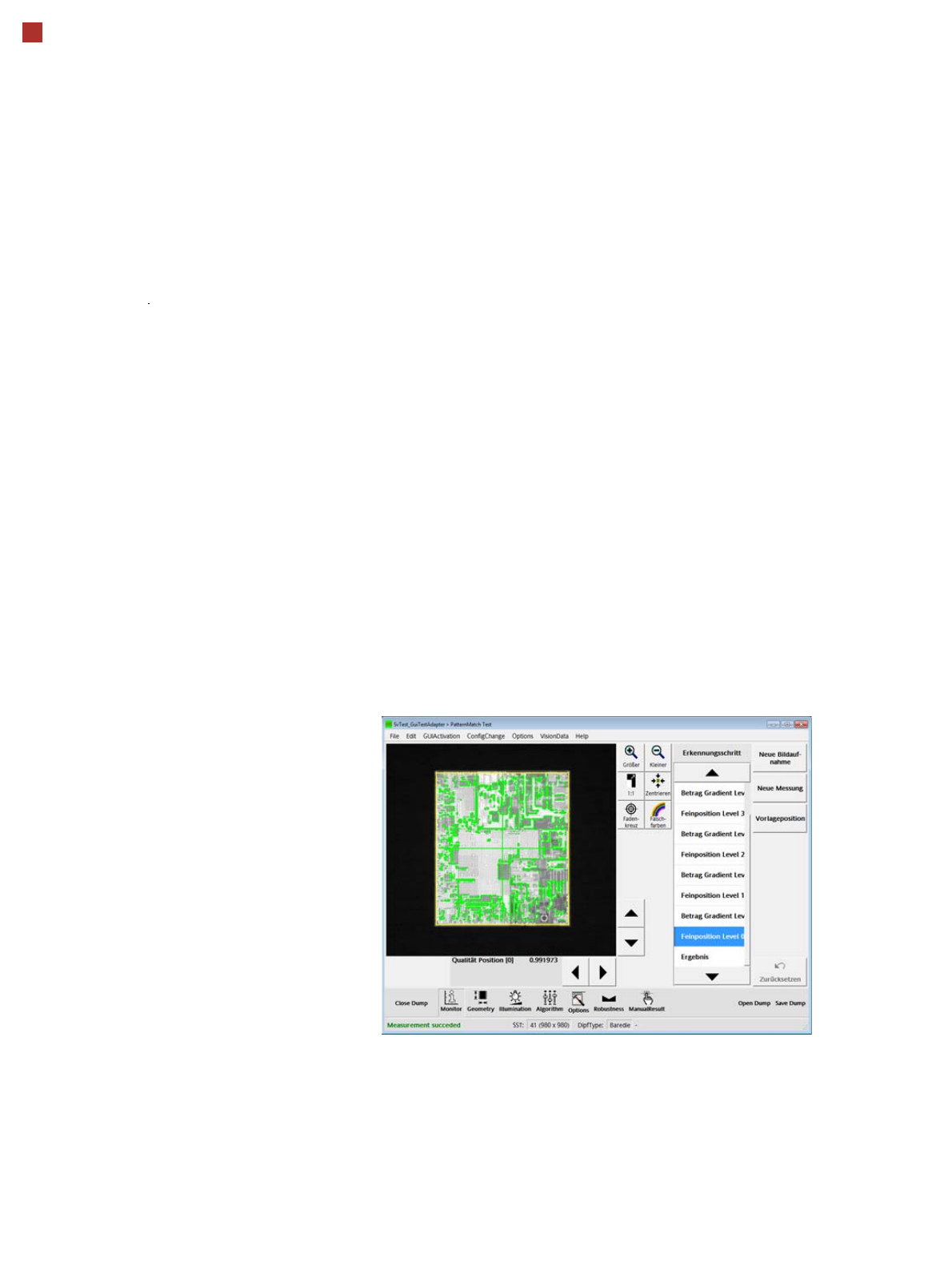
Pattern Matching
Pattern matching can be
used for components with
very fine contact pads, which
can not be detected with the
existing component camera
resolution. Searching and
detection is performed over a
larger area, which contains
unique structures (patterns).
Once the specified area has
been detected, the compo-
nent is aligned and placed
according to the position of
this area and in relation to the
substrate.

39
SIPLACE Vision
PCB position recognition
Fiducial criteria
Fiducial criteria
Locate 2 fiducials
Locate 3 fiducials
X-/Y-position, rotation angle, mean PCB distortion
Additional: shearing, distortion separately in X and Y direc-
tion
Fiducial shapes Synthetic fiducials: circle, cross, square, rectangle, dia-
mond, circular, square and rectangular contours, double
cross, pattern: any
Dimensions of patterns
Min. size
Max. size
0.5 mm
3 mm
Fiducial environment Clearance around reference fiducial not necessary if there
is no similar fiducial structure in the search area
Dimensions of synthetic fiducials
Min. X/Y size for circle and rectangle 0.25 mm
Min. X/Y size for annulus and rectangle 0.3 mm
Min. X/Y size for cross 0.3 mm
Min. X/Y size for double cross 0.5 mm
Min. X/Y size for diamond 0.35 mm
Min. frame width for annulus and rectangle 0.1 mm
Min. bar width / bar distance for cross, double-cross 0.1 mm
Max. X/Y size for all fiducial shapes 3 mm
Max. bar width for cross/double-cross 1.5 mm
Minimum tolerances generally 2% of nominal dimension
Max. tolerances generally 20% of nominal dimension