00193161-01.pdf - 第70页
Placement of 0 402 components Manual S-20/S-23 HM/S-25 HM/F4/F5 HM/HS-50 03/2001 edition 70 8.5 Checking the illumination values Å From the ‘ T est Componen t ’ men u (see Fig. 8 - 3 on page 62 ), cl ick on the ‘ Il lumi…
Manual S-20/S-23 HM/S-25 HM/F4/F5 HM/HS-50 Placement of 0402 components
03/2001 edition
69
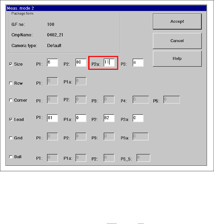
The error ‘Component length outside tolerance’ occasionally occurs with 0402 components. This
is generally caused by dirty nozzles.
It can also occasionally occur with 0402 components with a dark body and very narrow leads,
even though the nozzles are clean. In this case, you should change parameter P2a under ‘Size’
from 10 to 11.
Fig. 8 - 10 Measuring Mode 2 – Size mode parameter P2a modified
8.4 Checking the lead dimensions
Å From the ‘Test Component’ menu (see Fig. 8 - 3 on page 62), click on the ‘Lead Dimensions>’
button. The ‘Lead Dimensions’ video image appears, together with the parameters.
Å Check the set values
– optical length: 0.95 mm (up to 1 mm is possible)
– optical width: 0.45 mm (up to 0.5 mm is possible)
Å Press ESC to exit the ‘Lead Dimensions’ option.
Placement of 0402 components Manual S-20/S-23 HM/S-25 HM/F4/F5 HM/HS-50
03/2001 edition
70
8.5 Checking the illumination values
Å From the ‘Test Component’ menu (see Fig. 8 - 3 on page 62), click on the ‘Illumination’ button.
The ‘Illumination’ video image appears.
Å Use the ‘tab’ key to select the illumination level.
The brightness is displayed for each level. The values should be as follows:
Å Press ‘ESC’ to exit the ‘Illumination’ option and return to the main view.
9 Solder paste application
9.1 Mask printing
During solder paste printing with metal stencils, all the solder is deposited on a PCB in a single
pass. The solder paste is thoroughly mixed, and then ‘rolled’ over the metal stencil with the pattern
to be printed using a squeegee. The motion of the squeegee presses solder paste through the
apertures in the stencil and onto the PCB below.
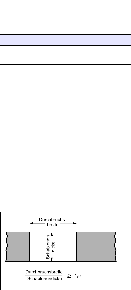
9.2 Properties of the stencil
Å Use a laser-cut stainless steel stencil for placing 0402 components, and note the following rule
of thumb for the shape of the apertures:
9
9
9
9
9
9
9
9
Fig. 9 - 1 Rule of thumb for the shape of the apertures
Illumination level Brightness
flat 120
average 100
steep 120

Manual S-20/S-23 HM/S-25 HM/F4/F5 HM/HS-50 Placement of 0402 components
03/2001 edition
71
PLEASE NOTE:
If you are not using laser-cut metal stencils and do not follow the rule of thumb for the shape of
the apertures, peaks of solder paste can form when you remove the stencil. 9
The solder paste is generally approximately 125 µm (5 mil) thick. If the apertures are of the wrong
shape or have rough surfaces, the adhesive strength of the solder paste increases, which means
that it does not easily come away from the walls of the aperture when the stencil is lifted. The
solder paste is then pulled up with the stencil. This can create peaks up to 300 µm high before the
solder paste finally tears away from the stencil.
If the stencils are too thick, the solder paste can ball together, thus causing short-circuits.
Recommendations for:
Stencil thickness / solder paste thickness150 µm (= 6 mil)
Stencil thickness / solder paste thickness125 µm (= 5 mil) 9
9.3 Solder paste
Standard solder paste generally has a grain size of 45 – 75 µm (type 3). To guarantee a smooth
and efficient placement process, we recommend the use of a fine pitch paste with a grain size of
20 - 45 µm (type 4).