AQ-2 spec book LR.pdf - 第12页
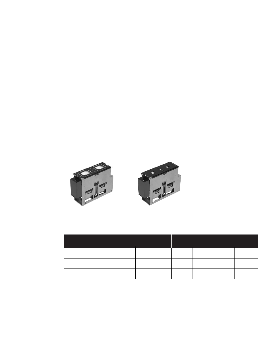
General Specifica tions 10 of 44 2.6 Board alignment T able 5 F igure 6 T he digital Board Alignment (BA) camer a (mounted on the H-Drive manipulator) is used to improv e the placement accuracy of the component with resp…
General Specifications
9 of 44
2.5 Component
vision
Figure 5
The Component vision (CV) system is used for the alignment of components on leads,
edges or bumps. Component Alignment is achieved by moving the placement head
above the lens of an upward-facing CV camera. A combination of multiple light sources
ensure sufficient contrast between the component (leads) and the background. Utilizing
these light sources (back light, dark field, mid field and bright field illumination) the
AQ-2 is capable of aligning almost any component. The illumination intensity is
automatically chosen based upon the reflectivity of the respective components. The CV
camera can determine the position of the component with respect to a reference plate.
The deviations, together with the fiducial alignment values, will be used to determine
the correct placement position.
There are two different component vision systems available for the AQ-2.
• The Component vision Large Field of View (LFOV) is used to align and inspect a wide
range of components up to 45 x45 mm or 66 x 23 mm with bump or lead width down
to 150 micron. It is also possible to inspect larger components but this can be done with
the component slightly above the focal plane of the camera allowing to inspect
components up to 165 x 45mm.
• The Component vision Small Field of View (CV SFOV) is used for ultra fine pitch
components like CSPs and flip chips. By use of a smaller field of view (22x22mm) a
higher accuracy can be achieved which is required for this type of components.
Components with bumps down to 80 micron with a 160 micron pitch can be measured.
Component vision modules
X-axis Y-axis Width Pitch Width Pitch
CV LFOV (mm) 45 45 0.150 0.300 0.150 0.300
CV SFOV (mm) 22 22 0.080 0.160 0.080 0.160
Component
vision Maximum component size Lead Bump
Table 4
Note: Component and lead dimensions above or below the noted specification require
an application review.
Note: Components larger than the noted field of view can be processed. For instance, the
CV LFOV can measure a 165mm long connector, however some restrictions may apply.
Also components of 66x23mm (or 23x66mm) can be measured in one view.
General Specifications
10 of 44
2.6 Board
alignment
Table 5
Figure 6
The digital Board Alignment (BA) camera (mounted on the H-Drive manipulator) is used
to improve the placement accuracy of the component with respect to the board by
measuring the global and/or local board fiducials or specific artwork features.
For PCBs that have no fiducials at all, the AQ-2 can make use of artwork recognition. The
board alignment camera can measure a specific part of the artwork of the PCB and
calculate the centre of that specific part of the PCB. For example, solder pads of a IC or
BGA can be used in this case.
Potential deviations (translation, rotation) are calculated with the data of the servo-
systems of the manipulator. The Board alignment system can also be used for bad mark
sensing. Board alignment is achieved by projecting light on the PCB and measuring the
intensity of the reflection with the use of a downward-facing camera.The dark surface of
the PCB only reflects a small amount of light. Traces of white copper or solder (lead)
reflect the light strongly. This contrast makes it possible to determine the position of the
substrate (fiducial or artwork marks). At least two points are required on the board to
determine its position. To achieve the highest accuracy, board stretch must be measured
and this requires at least three fiducials. Any fiducials or artwork, with sufficient
contrast, can be used.
Board alignment
Fiducial size (min.) 0.1mm
(max.) 4.0mm
Tolerance 20% of nominal
Clearance 2 x diameter of fiducial
Minimum contrast level 30%
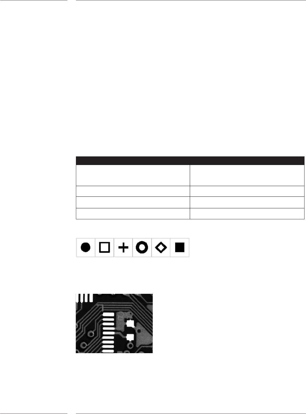
Samples of fiducial markers
Sample of artwork
Figure 7
General Specifications
11 of 44
2.7 User
Interfaces
2.8 Adaptive
pick-up
2.9 Continuous
Calibration
Figure 8
2.10 Bad mark
sensing
Table 6
A user-friendly touch screen on the front of the machine supports most of the operator
instructions (e.g. start, stop, error recovery, etc.). A keyboard supports all functions and
maintenance features at supervising and maintenance level.
Pick-up point correction can be used to calibrate the exact position at which components
should be picked. This can be achieved by manual or automatic correction. Manual pick-
up-point sensing lets the operator place the head above the component and save the
current head position as pick position. Auto correction can be applied to any component
using the digital vision system, the component vision results (delta x, delta y) are stored
and used to modify the pick-up location.
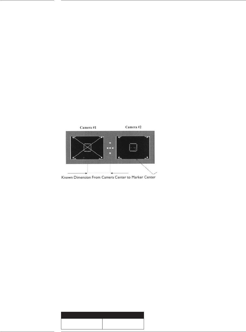
The AQ-2 System calibration is an on-line calibration that is performed automatically
with a reference plate each time a component is aligned.The glass reference plate, which
has a marker pattern on it, is fixed above the digital component alignment camera unit.
When the component camera system takes an image of a device, it automatically takes
an image of the reference pattern. Consequently the component camera system
measures the component with respect to this pattern.
Continuous calibration
Next to the placement head, the digital Board Alignment (BA) camera system is confi-
gured. At the same moment the component camera system takes an image of the
component and the reference pattern, the BA camera system takes an image of the head
marker as well. In this way the component position is measured with respect to the BA
camera system. Before component placement, the BA camera system has executed the
global board alignment which is used to relate the board coordinate system to the
machine coordinate system. Local fiducial or artwork alignment can be used to
determine more accurately where a fine-pitch component should be placed. This is
achieved by measuring an additional fiducial or artwork mark located near the
component placement position, prior to placement.
Bad mark sensing is used when multiple circuits are placed on one board. Markers that
contrast to the board surface can be used to identify circuits that do not need to be
assembled. The digital board alignment camera is used to scan these markers.
Components will not be placed onto circuits that have a bad mark present. The position
at which bad marks are located is programmable.
Optionally a master mark can be used. If this mark is present, it is assumed that one or
more circuits are bad, the AQ-2 will then scan all individual circuits. The position and use
of the master mark is programmable.
Bad marks
Minimum size >1mm