2023-0002-ITEC_003_Product-catalogue-Jan-2023_LR.pdf - 第10页
10 ITEC - PRODUCT PORTFOLIO Redu ce yo ur to t al co s t of o wne r ship. G ain quali t y insp ec t ion s and the e x ibilit y t o sc ale - wi tho ut comp ro mising on a ccur ac y, quali t y, o r spe ed . T he A DA T 3 …
9
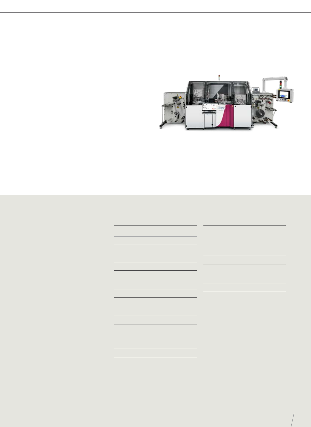
ADAT3 XF TAGLINER - HIGH-VOLUME RFID INLAY DIE BONDER
RFIDDIE ATTACH
Curing in milliseconds versus seconds in the current
industry practice, the ADAT3 XF Tagliner is three times
faster and 30% more accurate than anything on the
market. Common systems only work with transparent
web material; this Tagliner handles a diverse range,
including paper enabling you to move away from PET
plastics for sustainability. Eliminating manual handling
through automated wafer change and qualied for
die bond of all known ICs down to 200 μm die size, the
ADAT3 XF Tagliner performs a complete inspection
without sacricing speed and productivity.
For the highest productivity
and quality standard at the
lowest cost of ownership
Key features
Performance
• 48,000 units per hour with the machine
speed up to 50.8 mm web pitch
• High-precision die-attach
• Works with both transparent and
non-transparent web material
• High-precision glue dispense system
• High-speed thermal compression curing
system. Easy maintenance, one or two
units only
• 100% high-resolution optical inspections
on glue, die, attach and cure processes -
without compromising machine speed
• Process fully qualied for major chip
suppliers at the industry’s tightest
reliability requirements: temperature,
humidity, and mechanical
• 8 to 12 inches wafer compatible with
fully automatic wafer change
• Capable to handle dies down to 200 µm
• Single-track design for easy operation
and change over
• Integrated with BW Paper systems,
winding/conversion systems,
and Voyantic readers
Specications
Speed
• 48,000 units per hour ip chip
up to a web pitch of 50.8 mm
Die Range
• Die size: 200 x 200 µm to 5 x 5 mm
• Web width: 40 - 165 mm, single row
operation
Placement accuracy
• Die position: x, y: 1 σ < 9µm
• Die rotation: φ: 1 σ < 0.67°
• Pick and place force: 0.2 - 1.5 ± 0.1 N
Dispense accuracy
• Dot size accuracy: 1 σ < 10 µm
• Dot position accuracy: 1 σ < 10 µm
• Dot diameter: >200 µm
Cure system
• 2 stitch units, thermo compression cure
• Cure temperature range: 20 … 500 ± 5 °C
• Cure force range: 0 - 20 ± 0.5 N
• Cure time range: 0 - 5000 ms
QA vision inspections
• Glue dot size and -location
• Die top-side before attach
• Die bottom-side before attach
• Glue presence before attach
• Die presence before cure
• Die placement and rotation
Wafer handling
• 8 and 12 inches
• Steel/plastic Film Frame Carrier (FFC)
• Automatic wafer change
• Wafer expansion
• Automatic barcode reader
Subsystems
• BW Paper Systems
• Winder/Unwinder
• Voyantic Reader
Machine dimensions
• Length, width, height:
5397 x 1500 x 2617 mm
3
• Net weight: 5230 kg
10
ITEC - PRODUCT PORTFOLIO
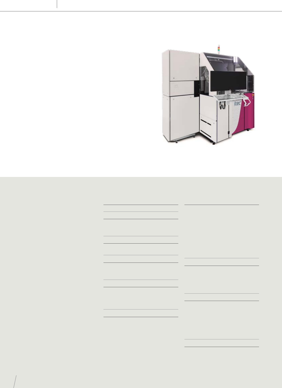
Reduce your total cost of ownership. Gain quality
inspections and the exibility to scale - without
compromising on accuracy, quality, or speed. The ADAT3
XF PiXelect Bonder is four times faster than anything on
the market - handling LED as small as 3x5 mil. The ip-chip
bin-mixing technology eliminates the sorting step and
manual wafer change. Multiple systems can be connected
- enabling you to build competitive, high-denition, and
cost-eective displays using mini-LED technology.
Ready for next-generation
LED direct view displays
ADAT3 XF PIXELECT BONDER - HIGH-SPEED HIGH-ACCURACY MINI-LED
BONDER WITH FLIP-CHIP FUNCTION
MINI-LEDDIE ATTACH
Key features
Performance
• Bonding 70,000 units per hour
• Handles the smallest LED sizes
on the market
• Flip and non-ip conguration
at same speed
• Standard deviation XY position
better than 3 μm
• Handles sorted as well as EPI wafer
input (sorting and bonding integrated
in one step)
• 100% high-resolution optical inspections
on die, attach, and post-bond steps
without compromising on machine speed
• 8 inches Film Frame Carrier (FFC) ring
with fully automatic wafer change
• Can be congured for manual load as well
as conveyor belt interface with a series
of systems (Red/Green/Blue (RGB) line)
• Can handle R, G, B colours in single
machine with placement gap down
to 20 μm
Specications
Speed
• 70,000 units per hour ip-chip bonding
Die Range
• Length, width: 75 x 125 μm to 2.5 x 2.5 mm
• Aspect Ratio: 1:1 - 1:3
• Thickness: 50 - 400 μm
Substrate range
• Minimum: 75 x 75 x 0.1 mm
• Maximum: 250 x 250 x 0.2 mm
Placement Accuracy
• Die position: x, y: 1 σ < 3µm
• Die rotation: φ: 1 σ < 1°
• Pick and place force: 0.2…1.5 ± 0.1 N
Pick up tooling
• Vespel collet
• Rubber tip
• Four-sided collet
• Push-up needle
Substrate Handling
• Manual
• Optional conveyor belt interface with
a series of machines (RGB line)
QA Vision Inspections
• Pre-pick inspection (wafer): Die alignment.
Frontside chipping. Wafer map alignment
• Pre-pick inspection (PKG carrier):
PKG alignment
• Frontside chipping. Carrier map alignment
• Post-pick (transfer): Die present.
Die alignment
• Pre-bond inspection on substrate:
Bond pad alignment
• Post-bond inspection incl. substrate
recognition: Die placement
Wafer handling
• Handling R, G, B wafers: EPI or Sorted
• 8 inches Film Frame Carrier (FFC) ring
• Automatic wafer change
• Wafer expansion
• Automatic barcode reader
Automation
• Full die traceability (full strip mapping)
• Auto recipe download (MES interface)
• Monitoring of critical process parameters
during production. Automatic stop function
when parameter out of control
• Servo, bond-force and vacuum auto-
diagnostics functionality to check health
status of the machine
Machine dimensions
• Length, width, height:
2050 x 1280 x 2100 mm
3
• Net weight: 1850 kg
11
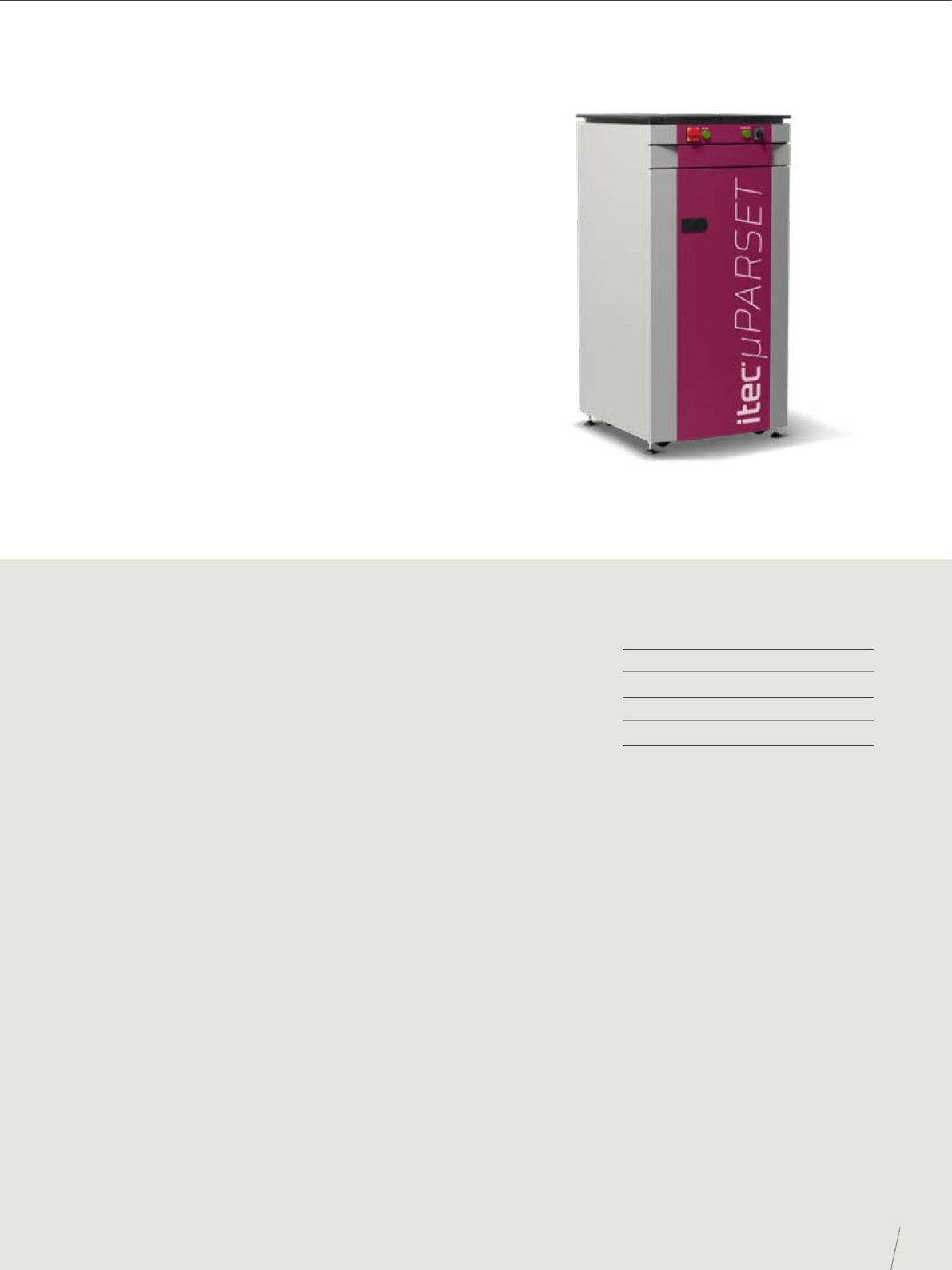
Eliminate power products’ lengthy test times for enhanced
output. This is the modular parameter test system for
power discrete semiconductor devices up to 12 leads.
The standard conguration has a maximum supply and
current per channel of 400V and 30A. Through its modular
architecture, this can be extended with a high voltage unit
of 2kV and a high current unit of 200A. µPARSET software
gathers data about measured devices and produces
various insights for product quality, stability, and yield
optimization.
The benchmark in analog
power testing
POWER µPARSET - DISCRETE POWER TESTER
TEST
Key features
Target segments
• Back-end nal test
• Wafer test
High performance
• Handler and prober agnostic
• 1 to 4 handlers
• Multi-site testing
• Short test times
• Pin electronics (voltage and current
measurement on all pins simultaneously)
• Maximum number of pins: (FT and AT/QT):
6 or 12 pins
• High-quality diagnostics and calibration
• High accuracy
• User-denable parameters
Test heads
• Current amplier for fast leakage
measurement
• Short and open pins close to DUT
• Dedicated test hardware
Embedded software
• User-denable parameters
• Visual ITEC: user-denable operator
interface
• Automatic multi-site expansion
• Scope function
• V and I waveforms and timing
on all channels
• Real-time diagnostics
• Curve traces
Specications
Maximum supply and current per channel
• 400 V / 30 A
Small footprint
• 600 x 665 x 1235mm
Other
• Extendable test heads for adding handlers
• Maximum: 12 leads
• Voltage: 220-240 VAC +/- 5%, 1-phase
• Current: Fused on 16 A
• Frequency: 50/60 Hz +/- 0.5 Hz
• Handler Interface: GPIB, TTL, RS232,
TCP/IP
• Optional SECS/GEM interface following
SEMI standard
Extendable software
• Equipment control for multiple test cells
• Post-processing
• Dynamic Part Average Test
• Static Part Average Test
• Moving Limits
• Nearest neighbourhood residual
Optional extension modules
• Qs: reverse recovery charge
(30 nC / 300 nC / 3 uC)
• Gate resistance and capacitance
(Rg/Cg) extension
• µPHV: high voltage test (2 kV)
• µPHC: high current unit (200 A)
• µPDI: digital interface 2 x 16 channels
fully oating
• SECS/GEM interface