2023-0002-ITEC_003_Product-catalogue-Jan-2023_LR.pdf - 第16页
T he Str ip -to - Str ip Insp ec t io n af te r plat ing gu aran te es t he quali ty o f W IP pr oduc t s wi t h fa st f e edba ck lo op. W he n manu fac tur ing c os t and quali t y ar e a conc er n, t he P HIX E L MIS …
Enhance your manufacturing eciency and
competitiveness with high-speed multi rows lead-frame
3D inspection, highly exible customizable design with
a simplex vision solution, and automatic high-speed
laser treatment for rejects. When cost and quality of
manufacturing are a concern, the 3D Post-Winbond
Reel-to-Reel Inspection guarantees the quality of die and
wire bond - enabling fast feedback loop. The PHIXEL DWR
minimizes waste and loss in manufacturing processes
- eliminating defects usually only discovered during the
electrical tests of nished products.
The only 3D inspection
solution in the market
for reel-to-reel products
15
Specications
Imaging system
• Cameras: 5 M pixels area camera
monochrome
• Number of cameras: 3
• Resolution/Field of view:
3.7 µm/pixel, FOV: 9 mm
• Minimum object detection: 15 µm
• Lighting: Compound lighting
Inspection categories
• Program mode: Fast programming
for common reject criteria
• Reject treatment: Electronic map
and laser
• Inspection view: Top and side view
Inspection items:
• Die defects: Foreign material.
Die placement. Glue on chip
• Wire defects: Ball shift. Sweep wire. Loop
height. Sagging wire. Stray wire. Broken
wire. Missing wire. Stitch o. Stitch oset
• Lead frame defects: Lead deformation.
Lead shift. Lead lift up. Missing chip
Key features
Application
• Inspection of lead-frame substrate to
detect post-die bond and wire bond defect
Key features
• High-speed fully auto wire loop/prole
inspection
• Min 5 MP camera for 3D inspection
• Laser cut option for reject handling
• Post-inspection after reject laser handling
• Inspection time: 7 µm resolution with
4cm/second
• SEMI standard with SECS/GEM interface
• Sophisticated defect mode classication
• Lead frame width 17 mm to 32 mm
• AOI cellular network architecture
for recipe and e-Map management
• Option: real-time data feeding to MES
and eSPC
• Option: auto email alert (defect/batch
summary)
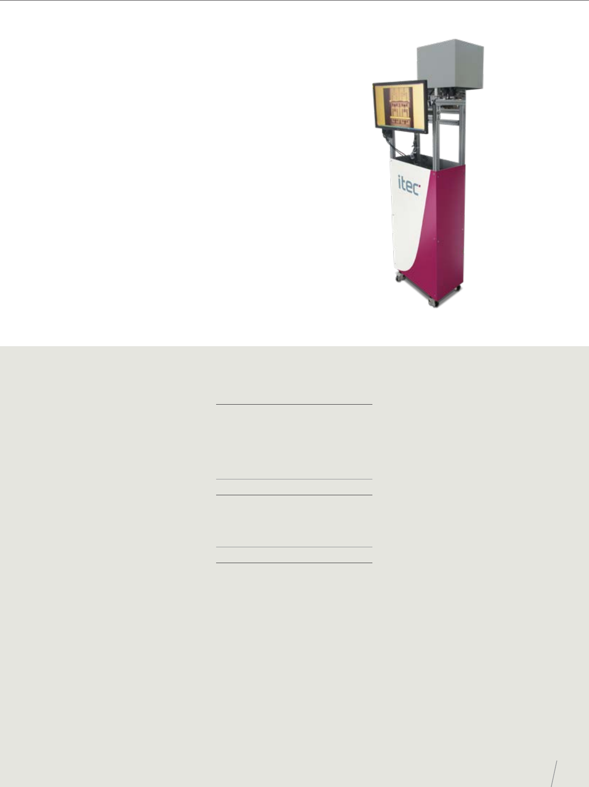
PHIXEL DWR - 3D POST-WIREBOND REEL-TO-REEL INSPECTION
OPTICAL INSPECTION
The Strip-to-Strip Inspection after plating guarantees the
quality of WIP products with fast feedback loop. When
manufacturing cost and quality are a concern, the PHIXEL
MIS minimizes waste and loss - enabling early detection
of defects usually only discovered during the nal 4th
Optical inspection of nished products. With ultra-high-
speed vision scan, high-precision for 2D inspection
DFN products, high accuracy laser for reject treatment,
and fast conversion, the PHIXEL MIS supports the largest
strip size: 100x300 mm.
Enables early detection
of production problems
to prevent loss
16
ITEC - PRODUCT PORTFOLIO
Specications
Imaging system
• Camera: 16K color line-scan camera
• Number of cameras: 2
• Resolution/Field of view: 3.17 to 6.3 µm /
pixel, FOV 50 mm to 100 mm
• Minimum object detection: 12 to 25 µm
• Lighting: Compound lighting
Inspection categories
• Program mode: Fast programming
for common reject criteria
• Reject treatment: Electronic map
and auto punching
• Inspection view: Top and bottom view
Inspection items
• Moulded lead-frame defects: Chipping.
Body broken. Scratch. Pin hole or void.
Mold shift. Incomplete mold. Gate remain.
Foreign material. Gate chipping. Rough
surface. Melted Body. Blister. Body crack.
Bubbles
• Lead-frame defects: Flash along lead. Cu
exposure. Contamination. Bend lead or
twisted lead. Mould compound leakage
on lead. Burr. Missing lead. U-shape ash
(mold ash under lead-frame). Indexing
hole deformation. Mold ash. Lead press.
Lead width. Empty (no encapsulation)
Key features
Application
• Inspection of lead-frame substrate
to detect package dimension,
molding and plating defect
Key features
• Dual stations for 2D inspection
and laser marker
• Throughput: 32,000 to 117,000 UPH
(subject to package size
& leadframe density)
• Support max 100 mm x 300 mm
substrate LF size
• 8K or 16K line scan camera resolution
• 3-4 magazines for on/o loaders
• Auto-lead frame QR code reading
• Full strip laser mark option
• Vacuum system and brush clean
for package laser mark
• AOI cellular network architecture
for recipe and e-Map management
• Option: real-time data feeding to MES
and eSPC
• Option: auto email alert (defect/batch
summary)
• SEMI standard with SECS/GEM interface
• Advanced Defect Classication (ADC) by
deep learning
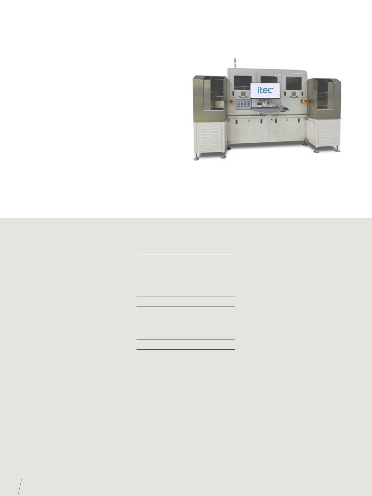
PHIXEL MIS - STRIP-TO-STRIP INSPECTION AFTER PLATING
OPTICAL INSPECTION
Work more eciently, productively, and accurately with
ultra-high-speed 2D vision inspection. This module is
built with automatic high-speed reject removal to prevent
sequence disruption. The PHIXEL CMR will guarantee your
products’ quality and eliminate product defects and eld
recalls - bringing customer complaints close to 0%.
The only equipment
on the market
providing full ePassport,
bankcard, and e-ID chipset
module inspection
17
Specications
Imaging system
• Imaging system
• Camera: 5M pixels area camera mono
• Number of cameras: 2 (top) + 1 (bottom)
• Resolution/Field of view: 12 µm/pixel
FOV:30 mm
• Minimum object detection: 48 µm
• Lighting: Compound lighting
Inspection categories
• Program mode: Fast programming
for common reject criteria
• Reject treatment: Electronic map
• Inspection view: Top and bottom view
Inspection items
• CDIF defects: Incomplete punch. Incorrect
punch. Contamination. Splicing connection
(distinguish colour, size, and location).
Mold void. Chipping. Die contamination.
Loose wire
• Chip module defects: Bend lead. Chipping.
Mold scratch. Gate remain. Mold
contamination. Crack. Lead scratch. Mold
ash. Incomplete ll. Scratch Ink mark.
Index hole deformation. Cold splicing.
Shift punch
Key features
Application
• Inspection of Contact/Contactless Dual
Interface (CDIF) module substrate to
detect encapsulated die, mold defect,
bonding wire, and plating defect
Key features
• Minimum 5MP colour camera for top
and bottom inspection
• 4 stations for 2D inspection, testing,
reject punch, and validation
• Throughput: up to 70,000 UPH
(subject to package size)
• Post-inspection after reject punch
• Zero balancing capability, total good,
and reject counts
• Customized AOI solution
• ID reader
• AOI cellular network architecture
for recipe and EMAP management
• Lead frame width: up to 35 mm
• SEMI standard with SECS/GEM interface
• Option: real-time data feeding to MES
and eSPC
• Option: auto email alert
(defect/batch summary)
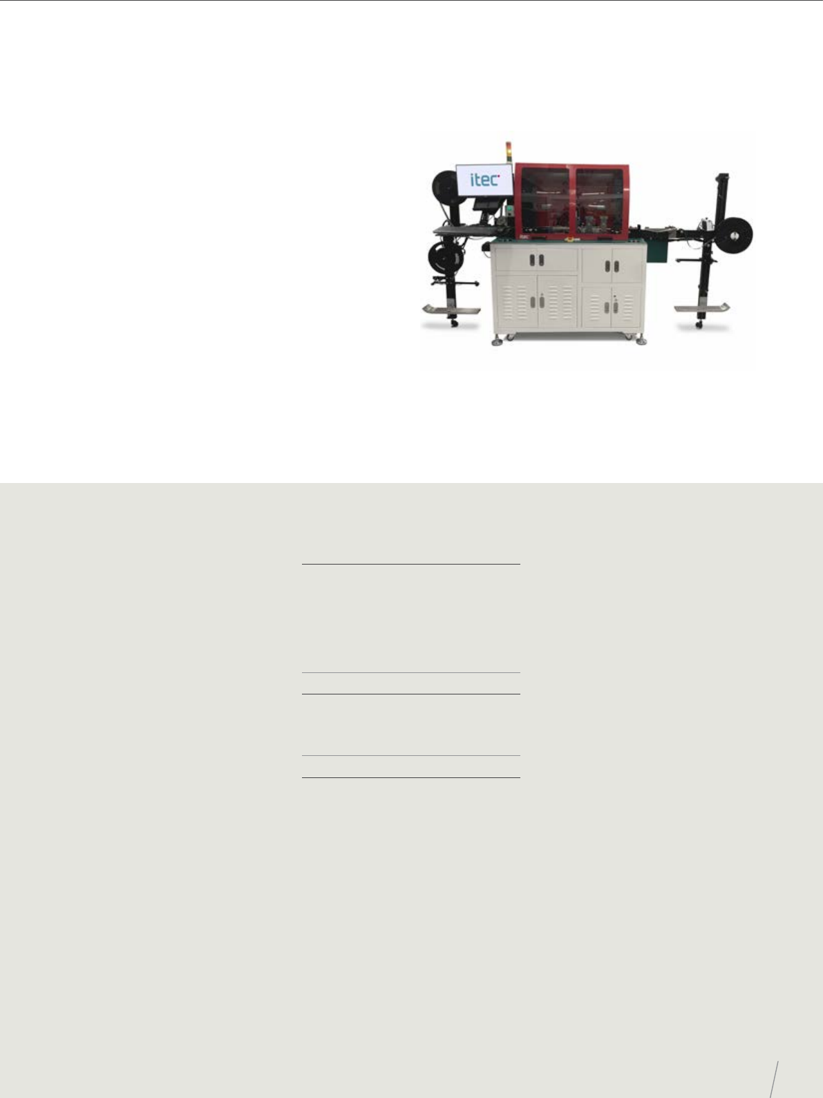
PHIXEL CMR - OPTICAL INSPECTION FOR CONTACT & CONTACTLESS MODULE
OPTICAL INSPECTION