2023-0002-ITEC_003_Product-catalogue-Jan-2023_LR.pdf - 第15页
Enhan ce your manu fa c tur ing e c iency and comp e ti t iv ene ss w it h high -s pe ed mul ti r o ws l ead -fr ame 3D insp ec t ion , highly e xibl e cus t omiz able de sign wi t h a simple x v isio n solu t ion , an…
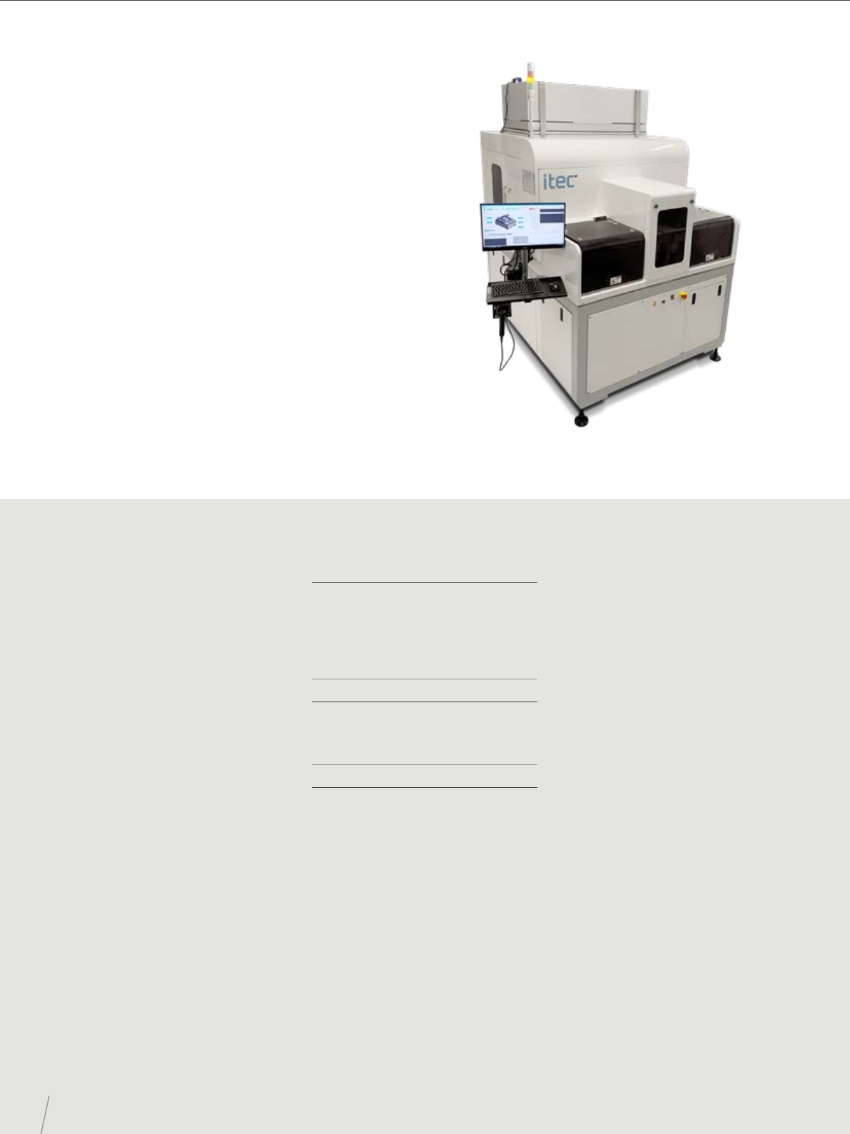
The most cost-ecient diced-wafer inspection system on
the market. With ultra-high-speed vision scan and high-
precision wafer 2D inspection, the Post Dicing Wafer AOI
enables conversion for 6”, 8”, and 12” wafer frame lm
carrier cassette. It guarantees the quality of diced wafer,
allows a fast feedback loop, and prevents wafer yield loss.
When cost and quality of manufacturing are a concern,
this diced-wafer inspection system oers a tight wafer
supply to eliminate wafer damage due to dicing issues.
WIF oers inspection after wafer dicing to detect surface
defects or inspection after package singulation of DFN to
detect package, mark, lead, and plating defects. Advanced
Defect Classication (ADC) by hybrid analysis will enhance
manufacturing eciency and competitiveness.
Minimize waste and
loss in the wafer
dicing process
14
ITEC - PRODUCT PORTFOLIO
Specications
Imaging system
• Camera: 16K line scan monochrome
• Number of cameras: 1
• 1.7 µm or 3.4 µm pixel resolution by pixel
binning
• Minimum object detection: 12 µm
• Lighting: Coaxial
Inspection categories
• Program mode: Fast programming
for common reject criteria
• Reject treatment: Electronic wafer map
• Inspection view: Top view
Inspection items
• Die related: Chipping. Damaged bump
larger than percentage of bump area. Bump
diameter. Shorted umps contact. Missing
bump. Scratch. Probe mark size larger than
percentage of bump area. Cracked die.
Kerf shifting. Discoloration
Key features
Application
• Inspection after wafer dicing to detect
surface defects
• Inspection after package singulation
to detect package,
mark, lead, and plating defects
Key features
• 2D surface inspection, stationary camera
• 128-thread processor
• 16K line scan camera resolution
• Supports high-density wafer up
to 500K dies
• FOV 25 mm with 2 magnications
selection or 0.85 µm by upscaled image
• Auto 2D barcode reading
• Hi-end vision performance
• High throughput at high-volume
manufacturing rate
• Granit base inspection work holder
• Supports 6”, 8”, 12” wafer
Automatic wafer map match
• Two cassettes at input loader
• SEMI standard with SECS/GEM interface
PHIXEL WIF - POST DICING WAFER AOI
OPTICAL INSPECTION
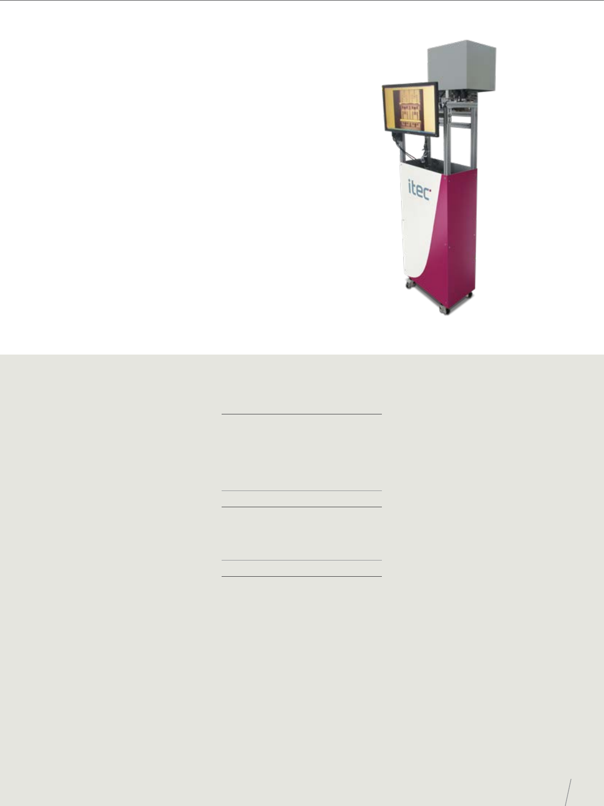
Enhance your manufacturing eciency and
competitiveness with high-speed multi rows lead-frame
3D inspection, highly exible customizable design with
a simplex vision solution, and automatic high-speed
laser treatment for rejects. When cost and quality of
manufacturing are a concern, the 3D Post-Winbond
Reel-to-Reel Inspection guarantees the quality of die and
wire bond - enabling fast feedback loop. The PHIXEL DWR
minimizes waste and loss in manufacturing processes
- eliminating defects usually only discovered during the
electrical tests of nished products.
The only 3D inspection
solution in the market
for reel-to-reel products
15
Specications
Imaging system
• Cameras: 5 M pixels area camera
monochrome
• Number of cameras: 3
• Resolution/Field of view:
3.7 µm/pixel, FOV: 9 mm
• Minimum object detection: 15 µm
• Lighting: Compound lighting
Inspection categories
• Program mode: Fast programming
for common reject criteria
• Reject treatment: Electronic map
and laser
• Inspection view: Top and side view
Inspection items:
• Die defects: Foreign material.
Die placement. Glue on chip
• Wire defects: Ball shift. Sweep wire. Loop
height. Sagging wire. Stray wire. Broken
wire. Missing wire. Stitch o. Stitch oset
• Lead frame defects: Lead deformation.
Lead shift. Lead lift up. Missing chip
Key features
Application
• Inspection of lead-frame substrate to
detect post-die bond and wire bond defect
Key features
• High-speed fully auto wire loop/prole
inspection
• Min 5 MP camera for 3D inspection
• Laser cut option for reject handling
• Post-inspection after reject laser handling
• Inspection time: 7 µm resolution with
4cm/second
• SEMI standard with SECS/GEM interface
• Sophisticated defect mode classication
• Lead frame width 17 mm to 32 mm
• AOI cellular network architecture
for recipe and e-Map management
• Option: real-time data feeding to MES
and eSPC
• Option: auto email alert (defect/batch
summary)
PHIXEL DWR - 3D POST-WIREBOND REEL-TO-REEL INSPECTION
OPTICAL INSPECTION
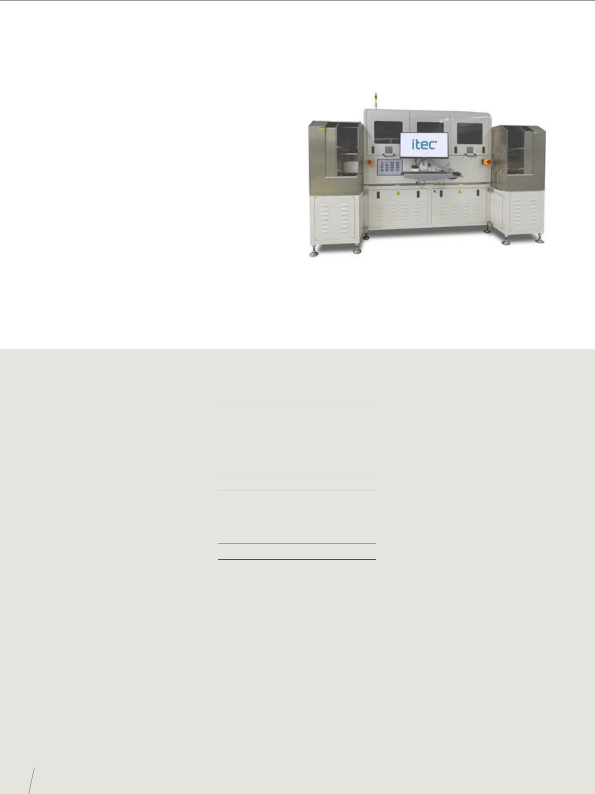
The Strip-to-Strip Inspection after plating guarantees the
quality of WIP products with fast feedback loop. When
manufacturing cost and quality are a concern, the PHIXEL
MIS minimizes waste and loss - enabling early detection
of defects usually only discovered during the nal 4th
Optical inspection of nished products. With ultra-high-
speed vision scan, high-precision for 2D inspection
DFN products, high accuracy laser for reject treatment,
and fast conversion, the PHIXEL MIS supports the largest
strip size: 100x300 mm.
Enables early detection
of production problems
to prevent loss
16
ITEC - PRODUCT PORTFOLIO
Specications
Imaging system
• Camera: 16K color line-scan camera
• Number of cameras: 2
• Resolution/Field of view: 3.17 to 6.3 µm /
pixel, FOV 50 mm to 100 mm
• Minimum object detection: 12 to 25 µm
• Lighting: Compound lighting
Inspection categories
• Program mode: Fast programming
for common reject criteria
• Reject treatment: Electronic map
and auto punching
• Inspection view: Top and bottom view
Inspection items
• Moulded lead-frame defects: Chipping.
Body broken. Scratch. Pin hole or void.
Mold shift. Incomplete mold. Gate remain.
Foreign material. Gate chipping. Rough
surface. Melted Body. Blister. Body crack.
Bubbles
• Lead-frame defects: Flash along lead. Cu
exposure. Contamination. Bend lead or
twisted lead. Mould compound leakage
on lead. Burr. Missing lead. U-shape ash
(mold ash under lead-frame). Indexing
hole deformation. Mold ash. Lead press.
Lead width. Empty (no encapsulation)
Key features
Application
• Inspection of lead-frame substrate
to detect package dimension,
molding and plating defect
Key features
• Dual stations for 2D inspection
and laser marker
• Throughput: 32,000 to 117,000 UPH
(subject to package size
& leadframe density)
• Support max 100 mm x 300 mm
substrate LF size
• 8K or 16K line scan camera resolution
• 3-4 magazines for on/o loaders
• Auto-lead frame QR code reading
• Full strip laser mark option
• Vacuum system and brush clean
for package laser mark
• AOI cellular network architecture
for recipe and e-Map management
• Option: real-time data feeding to MES
and eSPC
• Option: auto email alert (defect/batch
summary)
• SEMI standard with SECS/GEM interface
• Advanced Defect Classication (ADC) by
deep learning
PHIXEL MIS - STRIP-TO-STRIP INSPECTION AFTER PLATING
OPTICAL INSPECTION