2023-0002-ITEC_003_Product-catalogue-Jan-2023_LR.pdf - 第7页
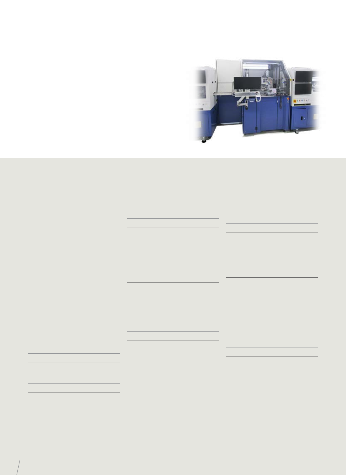
7 ADA T3XF DS - DIE SORTER (IN-LINE) DIE BONDER / DIE SORTER DIE A T T ACH Gain ma x imum pr oduc t i vi t y at t he lo we s t co st s . At 2 0 % fa st er t han any thin g in th e mark et, t his is t he die s or t er fo …
6
ITEC - PRODUCT PORTFOLIO
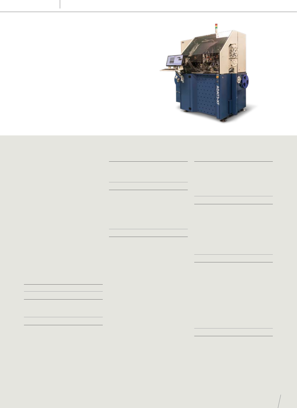
The only product in the market oering an in-line strip-
to-strip die bonder solution. The ADAT3 XF DBS receives
strips directly from one machine, processes them, and
feeds them to the next - maximizing your productivity.
Handling ultra-small and medium die at unparalleled
speed, it easily connects to top and bottom screen-
print equipment. This die bonder is also equipped with
automated wafer change and high-denition optics
for on-the-y quality inspection.
A breakthrough in cost,
quality, and productivity
ADAT3 XF DBS - HIGH-SPEED IN-LINE STRIP-TO-STRIP DIE BONDER
DIE BONDER / DIE SORTERDIE ATTACH
Key features
Performance
• Up to 60,000 units per hour
• Supports 8 to 12 inches wafer
on frame lm carrier
Strip size
• 100 x 300 mm
• Solder paste/Glue
•
Die size
• Minimal: 0.2 x 0.2 mm
• Maximum: 7 x 9 mm
• High throughput at high-volume
manufacturing rate
• Belt in, belt out
• Full die traceability (strip E142 – wafer)
• Auto recipe download: Manufacturing
Execution System (MES) interface
• SECS/GEM interface with E142
• Solder paste power application, SO8,
DPAK, and SOD123/128 SOT669
Specications
Speed
• Up to 60,000 units per hour (depending on
die size, lead frame pitch, glue/solder type
and selected quality inspections)
Die Range
• Length, width: 0.2 x 0.2 mm to 7 x 9 mm
• Aspect Ratio: 1:1 - 1:3
• Thickness: 50 - 400 µm
Lead frame size
• Minimum length, width: 100 x 40 mm
• Maximum length, width: 300 x 100 mm
• Thickness: 0.1 - 1.0 mm
System accuracy
• Small die (< 1 mm): XY: 1 σ xy ≤ 5 μm.
Rotation: 1 σ φ ≤ 1˚
• Large die (> 1 mm): XY: 1 σ xy ≤ 5 μm.
Rotation: 1 σ φ ≤ 0.3˚
• Pick and place force: 0.2-1.5 ± 0.1 N
Wafer handling
• Wafer size: 6 - 12 inches
• Wafer frame: 8 - 12 inches
• Steel/Plastic Film Frame Carrier (FFC)
• Foil Tension: programmable expander
(8 inches: 1 - 10 mm, 12 inches: 1 - 15 mm)
• Automatic wafer change and expander
• Automatic barcode reader
Lead frame handling
• Conveyor belt loading and unloading
according SMEMA protocol
Pick up tooling
• Vespel collet
• Rubber tip
• Four-sided collet
• Push-up needle
Imaging system
• Number of cameras: 4
• Resolution/Filed of View (FOV) glue: 0.3 MP
camera (3.2 UM/pixel), FOV 2.1 x 1.4 mm
• Resolution/ Filed of View (FOV) pick-up and
backside: 5.0 MP camera (2.3 UM/pixel),
FOV 5.6 x 4.7 mm
• Resolution/ Filed of View (FOV) post-bond:
5.0MP camera (4.6 UM/pixel), FOV 11.3 x
9.4 mm
• Resolution/ Filed of View (FOV)
sidewall: optional
• Minimal object detection:
10 micrometres (μm)
• Lighting: coaxial and ring light,
including multicolor light
Inspection categories
• Program mode: fast programming
for common reject criteria
• Reject treatment: strip map (E142)
and reject bin
• Inspection view: 4 cameras, (1) glue, (2)
pre-pick (3) back, (4) post-bond
Inspection items
• Die-related: Top chipping, backside
chipping. Damaged. Die size/die ratio.
Scratch. Cracked die. Discoloration
• Glue-related: Drop size. Drop shape
• Post-bond related: Die alignment
(position, size, rotation). Glue llet
Automation
• Wafer map SEMI E142 format,
SECS-GEM mpa exchange
• Start and reference die functionality
• Automatic Product Replacement
• MES Interface including auto recipe
download
• Monitoring of critical process parameters
during production. Automatic stop function
when parameter out of control
• Servo, bond-force and vacuum auto-
diagnostics functionality to check
health status of the machine
Machine dimensions
• Length, width, height:
2200 x 2100 x 1250 mm
3
• Net weight: 1950 kg
7
ADAT3XF DS - DIE SORTER (IN-LINE)
DIE BONDER / DIE SORTERDIE ATTACH
Gain maximum productivity at the lowest costs. At 20%
faster than anything in the market, this is the die sorter
for wafer-level CSP/micro CSP applications. It handles the
smallest die with automatic wafer change. The ADAT3 XF
DS also inspects all six sides of the die without any speed
penalty, securing quality in this critical last process step -
without compromising productivity or cost.
Future-ready for
next-generation die
Key features
Performance
• Up to 60,000 units per hour
• Supports 8 to 12 inches wafer
on frame lm carrier
Tape width
• 8 - 12 mm
• Sidewall inspection
Die size
• Minimal: 0.2 x 0.4 mm
• Maximal: 5 x 5 mm
• High throughput at high-volume
manufacturing rate
• APR auto-product replace
• In-tape inspection
• Automatic reel changer: optional
• Full die traceability: tape – wafer
• Auto recipe download (MES interface)
• SECS/GEM interface with E142
Specications
Speed
• Up to 60,000 units per hour ip or non-ip
Die Range
• Length, width: 0.4 x 0.2 mm to 5 x 5 mm
• Aspect Ratio: 1:1 - 1:3
• Thickness: 50 - 400 μm
Tape handling
• Width: 8 - 12 mm
• Pitch: 2 - 8 mm
• Thickness: 0.18 - 0.5 mm
• Tape specication: embossed carrier tape
with pocket hole, punch tape, paper tape,
surf tape
• Hot sealing: maximum temp 200 °C,
maximum force 10 - 80 Newton (N)
• Auto reel change, auto tape cutter
System accuracy
• Small die (< 1 mm): XY: 1 σ xy ≤ 5 μm.
Rotation: 1 σ φ < 1˚
• Large die (> 1 mm): XY: 1 σ xy ≤ 5 μm.
Rotation: 1 σ φ < 0.3˚
Wafer handling
• Wafer size: 6 - 12 inches
• Wafer frame: 8 - 12 inches
• Steel/Plastic Film Frame Carrier (FFC)
• Foil Tension: programmable expander
(8 inches: 1 - 10 mm, 12 inches: 1 - 15 mm)
• Automatic wafer change and expander
• Automatic barcode reader
Imaging system
• Number of cameras: 5
• Resolution/Field of View (FOV) pick-up
and backside: 5.0 MP camera
(2.3 UM/pixel), FOV 5.6 x 4.7 mm
• Resolution/ Field of View (FOV)
post-bond: 5.0MP camera (4.6 UM/pixel),
FOV 11.3 x 9.4 mm
• Resolution/ Field of View (FOV)
sidewall: 12.3MP camera (2.3 UM/pixel),
FOV 9.4 x 6.9 mm
• Resolution/ Field of View (FOV)
Die ON FLIP: 5.0 MP camera (2.3 UM/pixel),
FOV 5.6 x 4.7 mm
• Resolution/ Field of View (FOV)
post-seal inspection: 1.3 MP (3.7 UM/pixel)
FOV 9.7 mm
• Post-seal inspection: seal-line , index hole,
empty, tilted, body outline, product code,
marking, chipping
• Minimal object detection:
10 micrometres (μm)
• Lighting: red ring, coaxial,
and back panel light
Inspection categories
• Program mode: fast programming
for common reject criteria
• Reject treatment: strip-tape map (E142)
and reject bin
• Inspection view: 5 cameras, (1) pre-pick,
(2) back and sidewall, (3) front/bump,
(4) post-bond, (5) post-seal
Inspection items
• Die top-related: top chipping,
backside chipping
• Damaged. Die size/die ratio. Scratch.
Cracked die
• Discoloration. Bump inspections (size/
connected/missing)
• Backside related: Die alignment (position,
size, and rotation). Backside chipping
• Surface inspection: Punch through
inspection. Laser mark inspection. Pin A1
Automation
• Wafer map SEMI E142 format,
SECS-GEM mpa exchange
• Start and reference die functionality
• Automatic product replacement
• MES Interface including auto recipe
download
• Monitoring of critical process parameters
during production
• Automatic stop function when parameter
out of control
• Servo, bond-force and vacuum auto-
diagnostics functionality to check health
status of the machine
Machine dimensions
• Length, width, height:
2200 x 2100 x 1250 mm
3
• Net weight: 1850 kg
8
ITEC - PRODUCT PORTFOLIO
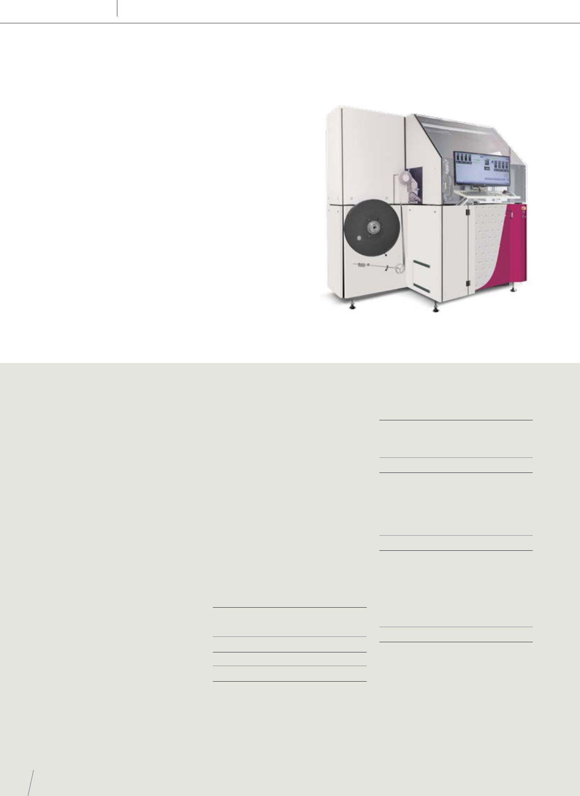
The Reel-to-Reel Eutectic Die Bonder supports all wafer
map formats and is designed with high-denition optics
for small-to-medium discrete products at extreme
speed. With die alignment, backside chipping, die size
measurement, and optional sidewall inspection for at
collets, the ADAT3 XF DBRE guarantees to enhance your
production, product quality, and total cost of ownership.
For a fully automated,
hands-o operation to increase
your uptime and output
ADAT3 XF DBRE - REEL-TO-REEL EUTECTIC DIE BONDER
DIE BONDER / DIE SORTERDIE ATTACH
Key features
Post-attach inspection
• Die present
• Lead frame alignment XY
• Black die detection
• Surface inspection as a roadmap element
Wafer handling
• Auto wafer change
• Wafer expansion
• Auto barcode reader
• Extensive wafer mapping and wafer
alignment functionality
Automation
• Wafer map formats: Market standards.
Full wafer map
• Wafer map alignment: Start and reference
die functionality.
• Auto equipment setup: via Semiconductor
Equipment Communication Standard
(SECS) / Generic Equipment Model (GEM)
• Traceability: ID input by barcode scanning
Specications
Speed
• 48,000 dies per hour with roadmap
to 60,000 dies per hour for small dies
(≤ 0.4 x 0.4 mm)
Product size
• 200 x 200 um to 5 x 5 mm
Lead frame size
• Up to 32 mm wide
Connectivity
• Connectivity via Semiconductor Equipment
Communication Standard (SECS) / Generic
Equipment Model (GEM) for automated
set-up and die traceability
• Automatic FFC wafer change for hands-o
operation (AEC-Q101 compliant)
• Flexible platform for all applications
• Fits in XF (Extended Flexibility) platform
architecture Reel-to-Reel lines
• Convertible to other XF (Extended
Flexibility) applications for leaded and
leadless to cater for product mix exibility
• Optional lead frame, anti-tarnish,
outgassing module
System accuracy
• Small die (≤ 0.4 x 0.4 mm)
• XY: 1 σ_xy ≤ 10 μm
• Rotation: 1 σ_φ < 1˚
Wafer handling
• Wafer diameter: 8 inches, 6 inches
on 8 inches Film Frame Carrier (FFC)
• Wafer frame: Steel Film Frame Carrier
(FFC) 8 inches or 12 inches
• Foil tension: 8 inches, 1 - 10 mm
• Wafer cassette: up to 25 slots
Die handling
• Process Temperature: maximum 470 °C
• Pickup force: 0.4 - 1.5 N ±0.1 N, Ultra-low
(programmable) pickup force (20 grams)
• Bond force: 0.2 - 1.5 N ±0.1 N
• Mixed gas: customer-specic
• Collet: pyramidal, at
• Ejector tool: single needle
Machine dimensions
• Machine length, width, height:
2050 x 1250 x 2200 mm
3
• Net weight: 1850 kg