2023-0002-ITEC_003_Product-catalogue-Jan-2023_LR.pdf - 第13页
13 Key f ea t ure s T ar ge t segmen ts • Ba ck- en d F inal Tes t • W a f e r Te s t • P C M Te s t High per f orm ance • Ne ar-zer o f oo t pr in t (2 13 x 4 4 0 m m) • Ul t ra - sh or t t e s t ti me s - inc re as ing…
12
ITEC - PRODUCT PORTFOLIO
Key features
Target segments
• Back-end nal test
• Wafer Test
High performance
• Handler and prober agnostic
• Multi-site testing
• 1 to 4 handlers
• Short test times
• Pin electronics (voltage and current
measurement
on all pins simultaneously)
• Maximum number of pins:
(FT and AT/QT): 6 or 12 pins
• High-quality diagnostics
and calibration
• High accuracy
Test heads
• Current amplier for fast leakage
measurement
• Short and open pins close to DUT
• Dedicated test hardware
Embedded software
• User-denable parameters
• Visual ITEC: user-denable operator
interface
• Automatic multi-site expansion
• Scope function
• V and I waveforms and timing
on all channels
• Real-time diagnostics
• Curve traces
Specications
Maximum supply and current per channel
• 400 V / 3 A
Small footprint
• 600 x 665 x 1235mm
Other
• Extendable test heads for adding
handlers (max 4)
• Maximum: 12 leads
• Voltage: 220-240 VAC +/- 5%, 1-phase
• Current: Fused on 16 A
• Frequency: 50/60 Hz +/- 0.5 Hz
• Handler Interface: GPIB, TTL, RS232,
TCP/IP
• Optional SECS/GEM interface following
SEMI standard
Extendable software
• Equipment control for multiple test cells
• Post-processing
• Dynamic part average test
• Static part average test
• Moving limits
• Nearest neighbourhood residual
Extreme exibility options:
• µPFM: oating mV meter
(30 mV / 300 mV / 3 V)
• DCM: digital capacitance meter
(0.3 / 3 / 30 / 300 pF)
• µMUX: multiplexer 4 x 24 pins
for multi-site test
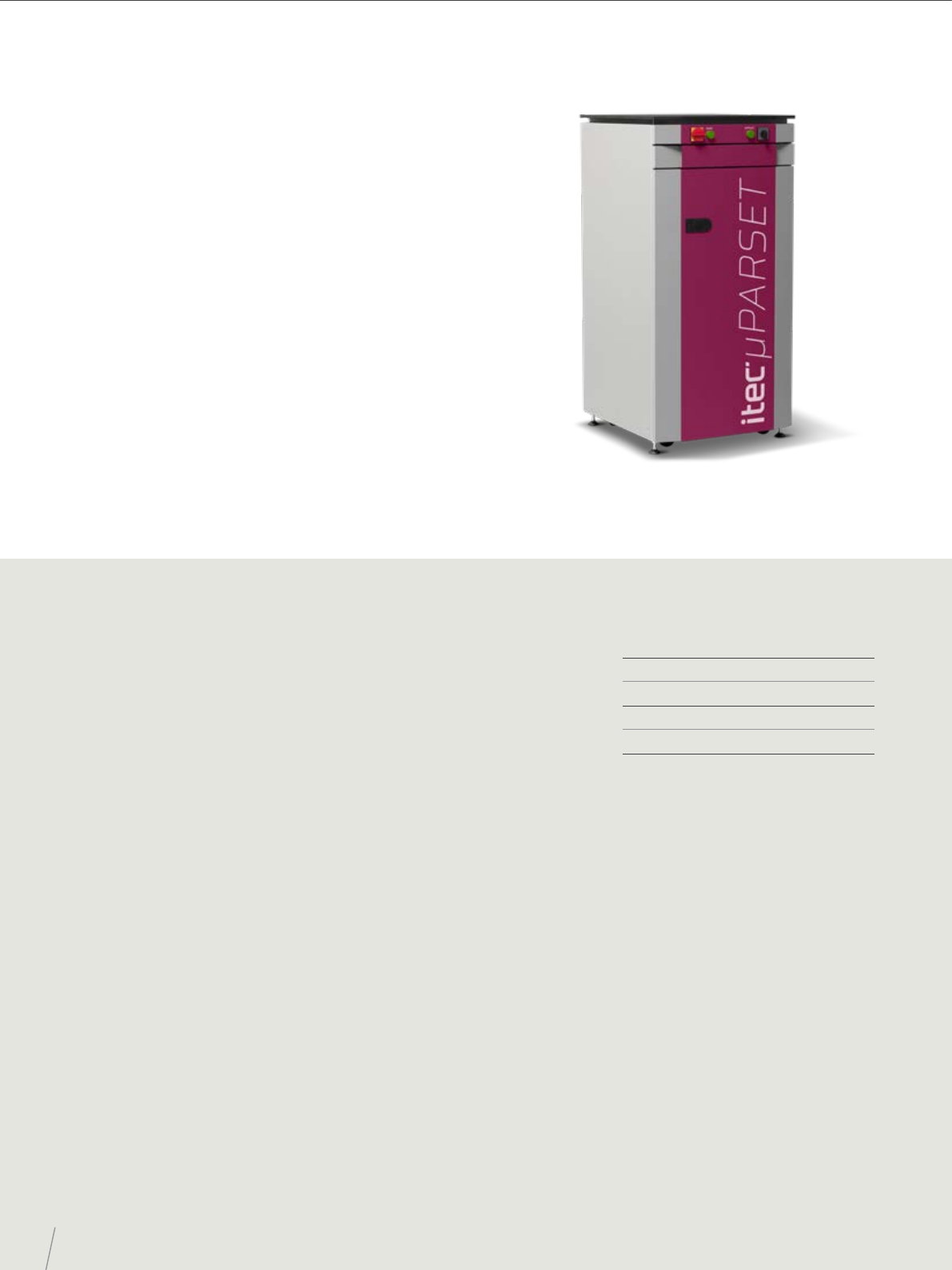
Gain short tester times and increase production at a lower
total cost of ownership. Built as a modular parameter test
system for discrete semiconductor devices with up to
12 leads, the Discrete High-Volume Tester enables high
throughput. Flexible hardware and software make
the Tester suitable for all wafer testing, nal testing,
acceptance or quality testing, and device characterization
tasks. µPARSET software gathers data about measured
devices and produces various insights. It is handler and
prober agnostic, equipped to connect to any prober or
tester. High accuracy leads to a narrow spread in test
results and better products. It can connect
up to four handlers when oor space is limited.
Eliminates lengthy
test times
µPARSET - DISCRETE HIGH-VOLUME TESTER
TEST
13
Key features
Target segments
• Back-end Final Test
• Wafer Test
• PCM Test
High performance
• Near-zero footprint (213 x 440 mm)
• Ultra-short test times - increasing UPH
• Highest accuracy in the market
• Extreme exibility
Multiple congurations possible with
• 1 booster controller (nTHBC)
• Up to 4 test heads (nSBTH)
with 6 channels
• Fast Kelvin check without switching relays
• Ultra-fast leakage test
• Pin electronics
• Multi-site testing
• Optional SECS/GEM interface following
SEMI standard
Embedded software
• User-denable parameters
• Visual ITEC: user-denable operator
interface
• Automatic multi-site expansion
• Scope function
• V and I waveforms and timing
on all channels
• Real-time diagnostics
• Curve traces
Specications
Maximum supply and current per channel
• 400 V / 3 A
Small footprint
• Test Head: 125 x 540 x 375 mm
• Booster: 213 x 440 x 875 mm
Other
• Extendable test heads for adding handlers
(up to 2 handlers)
• Maximum: 12 leads
• Voltage: 220 - 240 VAC +/- 5%, 1-phase
• Current: Fused on 16 A
• Frequency: 50 / 60 Hz +/- 0.5 Hz
• Handler Interface: GPIB, TTL, RS232,
TCP/IP
• Optional SECS/GEM interface following
SEMI standard
Extendable software
• Equipment control for multiple test cells
• Post-processing
• Dynamic Part Average Test
• Static Part Average Test
• Moving Limits
• Nearest neighbourhood residual
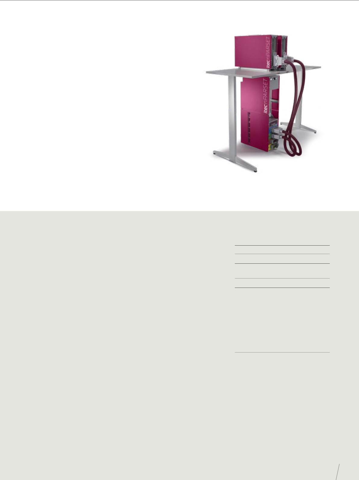
The most advanced modular parameter test system for
discrete semiconductors up to 6 or 12 leads. With ultra-
short test times, this tester is capable of testing up to
92000 devices per hour with a single test handler - the
fastest test cell on the market. This tester can be used as
a wafer tester, a PCM tester and as a nal tester in the
back-end. nanoParset occupies minimal oor space. Up
to four test heads can be combined as one to test 24-pin
packages at the highest possible throughput. Fast Kelvin
checks without switching relays to prevent breakage.
Eliminate long test times
and high-test costs
NANOPARSET - DISCRETE ULTRA-FAST TESTER
TEST
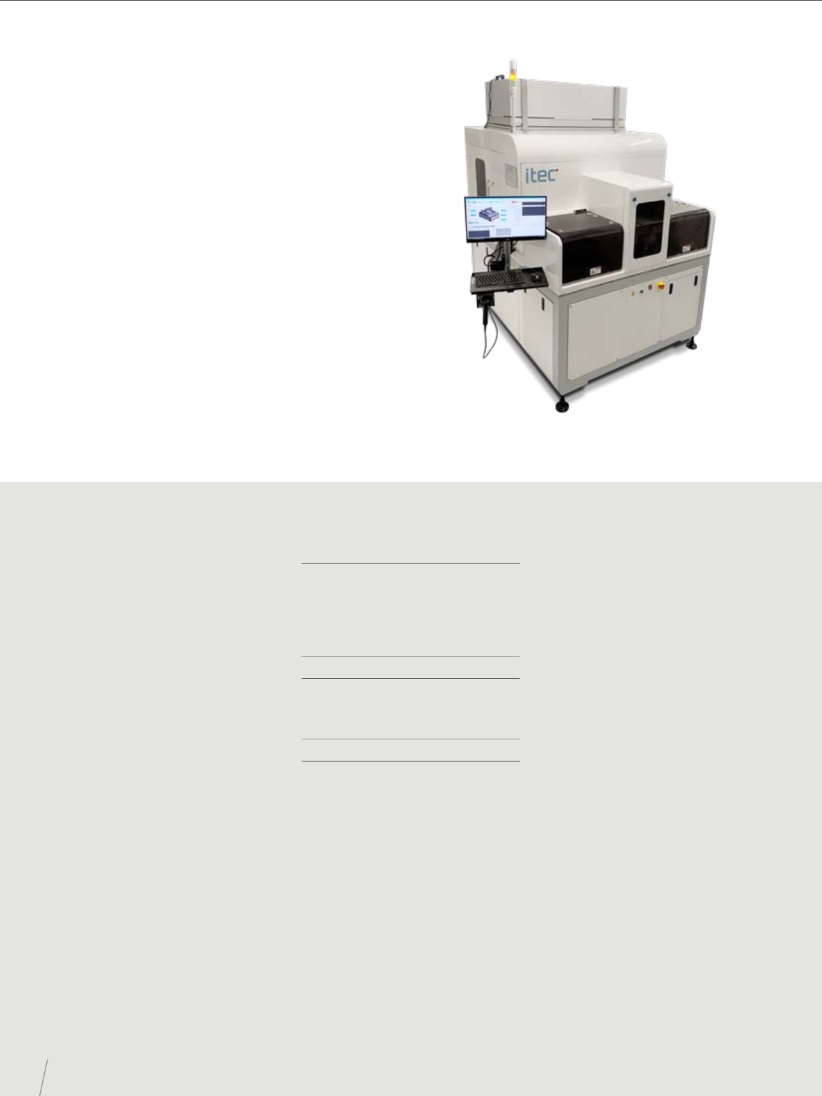
The most cost-ecient diced-wafer inspection system on
the market. With ultra-high-speed vision scan and high-
precision wafer 2D inspection, the Post Dicing Wafer AOI
enables conversion for 6”, 8”, and 12” wafer frame lm
carrier cassette. It guarantees the quality of diced wafer,
allows a fast feedback loop, and prevents wafer yield loss.
When cost and quality of manufacturing are a concern,
this diced-wafer inspection system oers a tight wafer
supply to eliminate wafer damage due to dicing issues.
WIF oers inspection after wafer dicing to detect surface
defects or inspection after package singulation of DFN to
detect package, mark, lead, and plating defects. Advanced
Defect Classication (ADC) by hybrid analysis will enhance
manufacturing eciency and competitiveness.
Minimize waste and
loss in the wafer
dicing process
14
ITEC - PRODUCT PORTFOLIO
Specications
Imaging system
• Camera: 16K line scan monochrome
• Number of cameras: 1
• 1.7 µm or 3.4 µm pixel resolution by pixel
binning
• Minimum object detection: 12 µm
• Lighting: Coaxial
Inspection categories
• Program mode: Fast programming
for common reject criteria
• Reject treatment: Electronic wafer map
• Inspection view: Top view
Inspection items
• Die related: Chipping. Damaged bump
larger than percentage of bump area. Bump
diameter. Shorted umps contact. Missing
bump. Scratch. Probe mark size larger than
percentage of bump area. Cracked die.
Kerf shifting. Discoloration
Key features
Application
• Inspection after wafer dicing to detect
surface defects
• Inspection after package singulation
to detect package,
mark, lead, and plating defects
Key features
• 2D surface inspection, stationary camera
• 128-thread processor
• 16K line scan camera resolution
• Supports high-density wafer up
to 500K dies
• FOV 25 mm with 2 magnications
selection or 0.85 µm by upscaled image
• Auto 2D barcode reading
• Hi-end vision performance
• High throughput at high-volume
manufacturing rate
• Granit base inspection work holder
• Supports 6”, 8”, 12” wafer
Automatic wafer map match
• Two cassettes at input loader
• SEMI standard with SECS/GEM interface
PHIXEL WIF - POST DICING WAFER AOI
OPTICAL INSPECTION