2023-0002-ITEC_003_Product-catalogue-Jan-2023_LR.pdf - 第4页
4 ITEC - PRODUCT PORTFOLIO Fr om f as t, accur at e die b onder s an d sor t er s f or mas s- pr odu ced s emic onduc t or d ev ice s , t o high-t hr oughpu t pr oduc ti on te s te r s and highly e c ient A u to mat ed …

3
ITEC’s goal is to increase our market presence fourfold by 2027.
Through disruptive innovations we enable our customers to
address the current semiconductor boom in a sustainable way.
Our solutions redene semiconductor manufacturing by pushing
the boundaries of speed with uncompromised quality and
lowest cost. We are growing our R&D centers in Nijmegen in the
Netherlands and Hong Kong, and we’re looking to expand further
into Asia with a manufacturing site in China, which will increase
our responsiveness and eciency even more.
Marcel Vugts,
ITEC General Manager

4
ITEC - PRODUCT PORTFOLIO
From fast, accurate die bonders and sorters for mass-produced semiconductor devices, to high-throughput production
testers and highly ecient Automated Optical Inspection (AOI) systems. ITEC gives you a competitive technological
edge in semiconductor manufacturing.
A PORTFOLIO
OF ADVANCED
SOLUTIONS
DIE ATTACH
ITEC’s XF ADAT3 platform is one of the most versatile die
attach solutions for semiconductor, LED display and RFID-inlay
manufacturing. There is a range of options to tailor the solution
to our customer`s needs, including Strip-to-Strip (Glue / DAF /
Eutectic), Reel-to-Reel, (Eutectic) and Flip-Chip.
Optimized for key markets
Semiconductors
The ADAT3 XF is combining high productivity, high
quality and the lowest cost of ownership with a record-
breaking-output all the way up to the 60,000 UPH
for die bonding and sorting applications.
RFID Inlays
With the ADAT3 XF Tagliner capable of 48,000 UPH
ITEC brings its proven technology to the RFID inlay
market enabling a productivity breakthrough at high
quality and low maintenance.
Mini/Micro LED Displays
While speed is key, placement accuracy is essential
when it comes to stitching together LED displays
And ITEC’s 70,000 UPH ADAT3 XF miniLED die bonder
delivers on both counts.
ACCURATE HIGH-SPEED
PRODUCTION TESTERS
In the world of high-speed semiconductor production
testers, the ITEC’s Parset family has set the standard
for discrete testing for the last 30 years. Consisting of
three models - µParset, Power µParset, nanoParset,
these fastest discrete testers are exible and extendable.
Every model in the range works seamlessly with any
handler and wafer prober, and with the fastest test-times
in the market the nanoParset already enables ultra-fast
handlers (UPH > 90,000).
AUTOMATED OPTICAL INSPECTIONS
Front-end and back-end semiconductor productivity can
be signicantly improved by smart implementation of
the best Advanced Optical Inspection (AOI) equipment
at critical inspection points in your production lines. ITEC
oers inspection solutions for 2nd Optical, 3rd Optical,
4th Optical, mid-end inspection (after mold & plating)
and for chip modules too, both inline and standalone.
ITEC combines deep learning and traditional algorithm in
machine vision to ensure the highest quality.
SMART MANUFACTURING
Ensuring your production with the automotive quality
and the highest yield against the lowest total cost-of-
ownership is ITEC’s playground. The ITECore automation
and smart manufacturing software suite is key to
extracting the maximum productivity from your back-end
semiconductor tools and platforms.
5
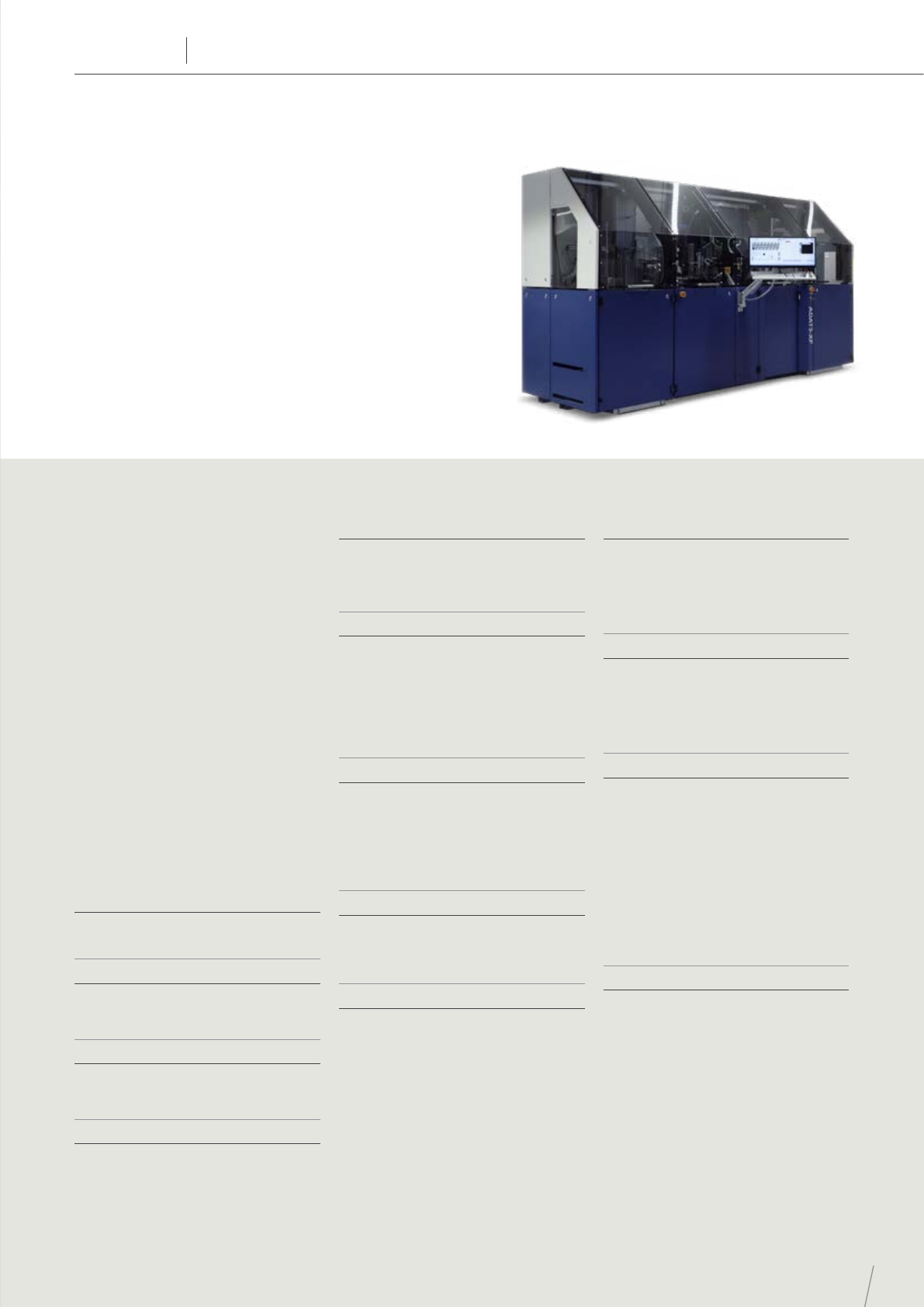
ADAT3 XF DBSG - STRIP GLUE DIE BONDER
DIE BONDER / DIE SORTERDIE ATTACH
Eliminate the trade-o between quality and productivity
with high-denition inspection executed on the y
without any speed penalty. At four times faster than
anything on the market, this is the industry’s leading
strip-to-strip die bonder for leaded or leadless packages
with glue or DAF/WBC applications. The ADAT3 XF DBSG
eliminates manual wafer change and speed drop, plus is
capable of handling die as small as 0.2 x 0.2 mm.
Future-ready for
next-generation dies
Key features
Performance
• Up to 60,000 units per hour
• Supports 8 to 12 inches wafer
on frame lm carrier
Strip size
• 100 x 300 mm
• Glue/DAF/WBC
Die size
• Minimal: 0.2 x 0.2 mm
• Maximum: 5 x 5 mm
• High throughput at high-volume
manufacturing rate
• 4 cassettes at output or optional
at input autoloader
• Full die traceability (strip E142 – wafer)
• Auto recipe download (MES interface)
• SECS/GEM interface with E142
• QFN, DFN, HVQFN, SOT, SO, TSSOP,
LGA leadless and leaded packages
Specications
Speed
• Up to 60,000 units per hour, depending
on die size, lead frame pitch, glue type
and selected quality inspections
Die Range
• Length, width: 0.2 x 0.2 mm to 5 x 5 mm
• Aspect Ratio: 1:1 - 1:3
• Thickness: 50 - 400 um
Lead frame size
• Minimum length, width: 100 x 40 mm
• Maximum length, width: 300 x 100 mm
• Thickness: 0.1 - 1.0 mm
System accuracy
• Small die (≤ 1 mm): XY: 1 σ xy ≤ 5 μm.
Rotation: 1 σ φ ≤ 1˚
• Large die (> 1 mm): XY: 1 σ xy ≤ 5 μm.
Rotation: 1 σ φ ≤ 0.3˚
• Pick and place force: 0.2 - 1.5 ± 0.1 N
Inspection categories
• Program mode: fast programming
for common reject criteria
• Reject treatment: strip map (E142)
and reject bin
• Inspection view: 4 cameras, (1) glue,
(2) pre-pick, (3) back, (4) post-bond
Inspection items
• Die-related: top chipping, backside chipping.
Damaged. Die size/die ratio. Scratch.
Cracked die. Discoloration
• Glue-related: Drop size. Drop shape
• Post-bond related: Die alignment
(position, size, rotation). Glue llet
Automation
• Wafer map SEMI E142 format,
SECS-GEM MPA exchange
• Start and reference die functionality
• Automatic Product Replacement
• MES Interface including auto recipe
download
• Monitoring of critical process parameters
during production. Automatic stop function
when parameter out of control
• Servo, bond-force and vacuum auto-
diagnostics functionality to check
health status of the machine
Machine dimensions
• Length, width, height:
3000 x 2100 x 1250 mm
3
(without magazine loader)
• Length, width, height:
3500 x 2100 x 1250 mm
3
(with magazine loader)
• Net weight: 3000 kg
(without magazine loader)
• Net weight: 3300 kg
(with magazine loader)
Pick up tooling
• Vespel collet
• Rubber tip
• Four-sided collet
• Push-up needle
Wafer handling
• Wafer size: 6 - 12 inches
• Wafer frame: 8 - 12 inches
• Steel/Plastic Film Frame Carrier (FFC)
• Foil Tension: programmable expander
(8 inches: 1-10 mm; 12 inches: 1 - 15 mm)
• Automatic wafer change and expander
• Automatic barcode reader
Lead frame handling
• Stack loader including paper separation
• Magazine loader/unloader: maximum
4 magazines at load and unload 20 - 40
slots per
• Magazine size: Minimum length, width,
height: 100 x 45 x 80 mm. Maximum length,
width, height: 305 x 110 x 270 mm
Dispense
• Twin cross writing module,
volumetric dispense
• Dot/Cross size, resolution: ≥ 250 um 1 σ 10 µm
• Dot/Cross position: 1 σ ≤ 20 µm
Imaging system
• Number of cameras: 4
• Resolution/Field of View (FOV) glue: 0.3 MP
camera (3.2 UM/pixel), FOV 2.1 x 1.4 mm
• Resolution/ Field of View (FOV) pick-up
and backside: 5.0 MP camera (2.3 UM/
pixel), FOV 5.6 x 4.7 mm
• Resolution/ Field of View (FOV) post-bond:
5.0MP camera (4.6 UM/pixel), FOV 11.3 x
9.4 mm
• Resolution/ Field of View (FOV) sidewall:
optional
• Minimal object detection:
10 micrometres (μm)
• Lighting: coaxial and ring light,
including multicolour light