2023-0002-ITEC_003_Product-catalogue-Jan-2023_LR.pdf - 第18页
Guar ant ee s t he quali ty o f t he pr o duc t s you p ro duce and deli ver. Th e Po s t-Se al In- T ap e Insp ec t ion eli minat e s quali ty d ef ec t s - br inging cu st ome r comp laint s and eld re c all ra te s …
Work more eciently, productively, and accurately with
ultra-high-speed 2D vision inspection. This module is
built with automatic high-speed reject removal to prevent
sequence disruption. The PHIXEL CMR will guarantee your
products’ quality and eliminate product defects and eld
recalls - bringing customer complaints close to 0%.
The only equipment
on the market
providing full ePassport,
bankcard, and e-ID chipset
module inspection
17
Specications
Imaging system
• Imaging system
• Camera: 5M pixels area camera mono
• Number of cameras: 2 (top) + 1 (bottom)
• Resolution/Field of view: 12 µm/pixel
FOV:30 mm
• Minimum object detection: 48 µm
• Lighting: Compound lighting
Inspection categories
• Program mode: Fast programming
for common reject criteria
• Reject treatment: Electronic map
• Inspection view: Top and bottom view
Inspection items
• CDIF defects: Incomplete punch. Incorrect
punch. Contamination. Splicing connection
(distinguish colour, size, and location).
Mold void. Chipping. Die contamination.
Loose wire
• Chip module defects: Bend lead. Chipping.
Mold scratch. Gate remain. Mold
contamination. Crack. Lead scratch. Mold
ash. Incomplete ll. Scratch Ink mark.
Index hole deformation. Cold splicing.
Shift punch
Key features
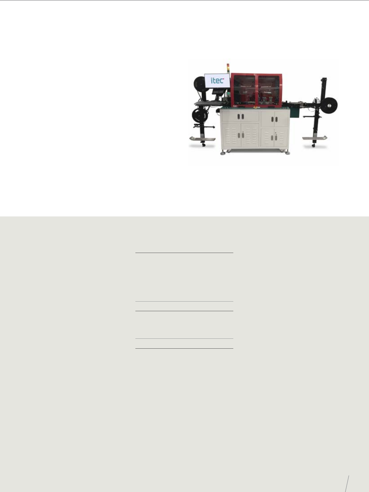
Application
• Inspection of Contact/Contactless Dual
Interface (CDIF) module substrate to
detect encapsulated die, mold defect,
bonding wire, and plating defect
Key features
• Minimum 5MP colour camera for top
and bottom inspection
• 4 stations for 2D inspection, testing,
reject punch, and validation
• Throughput: up to 70,000 UPH
(subject to package size)
• Post-inspection after reject punch
• Zero balancing capability, total good,
and reject counts
• Customized AOI solution
• ID reader
• AOI cellular network architecture
for recipe and EMAP management
• Lead frame width: up to 35 mm
• SEMI standard with SECS/GEM interface
• Option: real-time data feeding to MES
and eSPC
• Option: auto email alert
(defect/batch summary)
PHIXEL CMR - OPTICAL INSPECTION FOR CONTACT & CONTACTLESS MODULE
OPTICAL INSPECTION
Guarantees the quality of the products you produce
and deliver. The Post-Seal In-Tape Inspection eliminates
quality defects - bringing customer complaints and eld
recall rates close to 0 PPM. The PHIXEL IHW has a fast
convertible for 7-13-inch” carrier tape reel diameter and
auto conversion for dierent carrier tape widths up to
32mm. With AOI cellular network architecture for recipe
management and Advanced Defect Classication (ADC)
by hybrid analysis, the Post-Seal In-Tape Inspection
outperforms market competition to go above and
beyond your customers’ requirements.
The only post-tape
inspection equipment on
the market providing full
inspection capability
18
ITEC - PRODUCT PORTFOLIO
Specications
Imaging system
• Camera: 5M pixels area camera
monochrome
• Number of cameras: 2: 1 (top) + 1 (bottom)
• Resolution/Field of view: 4 - 16 µm/pixel
FOV: 10 mm to 40 mm
• Minimum object detection: 16 µm
• Lighting: Compound lighting
Inspection categories
• Program mode: Fast programming
for common reject criteria
• Reject treatment: Electronic map
• Inspection view: Top (and angle camera
for lead lift-up defect as upgrade option)
Key features
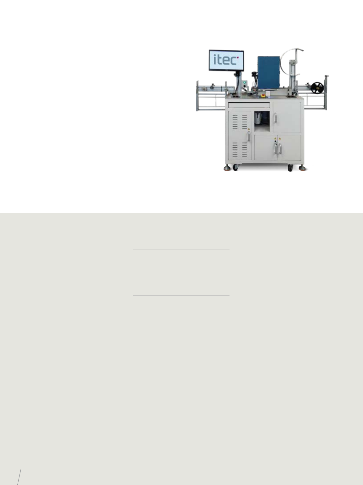
Application
• Inspection after taping to detect
orientation, lead, mark, seal, package
surface defect, reel label and quantity
Key features
• Min. 5 MP camera for top & bottom
inspection
• AOI cellular network architecture
for recipe management
• Reel size: 7” to 13”
• Throughput: up to 120,000 UPH
(subject to package size & pitch)
• Option: tilted lead defect vision
• Cu exposure detection under development
• Package: leaded, leadless, and WLCSP
• Carrier tape width: 8 to 32 mm
(auto track width)
• Advanced Defect Classication (ADC)
• SEMI standard with SECS/GEM interface
• Option: real-time data feeding to MES
and eSPC
• Option: auto email alert (defect/batch
summary)
Inspection items
• Marking defects: Unclear mark (faded
character). Shift mark (misaligned
marking). Incomplete mark. Double mark
(multiple character). Vertical mark (wrong
orientation). No mark. Mixed marking
• Moulded Package defects: Bubbles/
bulge. Voids/pin holes. Crack. Broken body.
Chipping Scratch. Unmoulded. Incomplete
ll. Foreign material
• Lead Package defects: Mould ash
on/along lead. Foreign material and
contamination. Exposed wire/clip. Ejector
mark. Visible wire Solder bridging. Bent
lead/lead angle. Lead sweep. Lead length.
Lead spacing/span. Lead cuts/depressions/
damage. Lead burr. Missing lead. Lead
length. Incomplete lead forming. Metal burr
• Taping defects: Loose/unseal cover tape.
Cover tape misalignment. Damaged/
contamination cover tape. Deformed/
damaged cavity. Damaged bottom tape.
Chipped/broken body. Mixed product. Edge
sealing. Unseal tape. Oset sealing.
• Cover tape tearing. Product tilting
PHIXEL IHW - POST-SEAL IN-TAPE INSPECTION
OPTICAL INSPECTION

19
NIJMEGEN
Jonkerbosplein 52
6534 AB Nijmegen
The Netherlands
HONG KONG
Unit HL-G01 G/F, Building
22E, Phase 3, Hong Kong
Science Park, Pak Shek
Kok, Shatin, Hong Kong
The iconic FiftyTwoDegrees building, which stands
next to the Novio Tech Campus in Nijmegen is the
headquarters of ITEC. This eectively takes the company
back to its roots where the rst diodes were created in
1953. Besides our headquarters in Nijmegen, ITEC has
an oce in Hong Kong for supply chain management
and customer support. We also have representatives
in multiple countries.
Global solutions,
local support
Would you like to talk to one of our specialists and
discover how our solutions can help your business?
Get in touch: info@ITECequipment.com
GET IN TOUCH!
GERMANY
MALAYSIA
JAPAN
PHILIPPINES
FRANCE
CHINA
CHINA
INDIA
THAILAND
TAIWAN
WAFER FAB
BACK-END FACTORY
UK
WE SERVE OUR CLIENTS
ACROSS 10 COUNTRIES: