Specification SIPLACE CA-Series2014版.pdf - 第24页
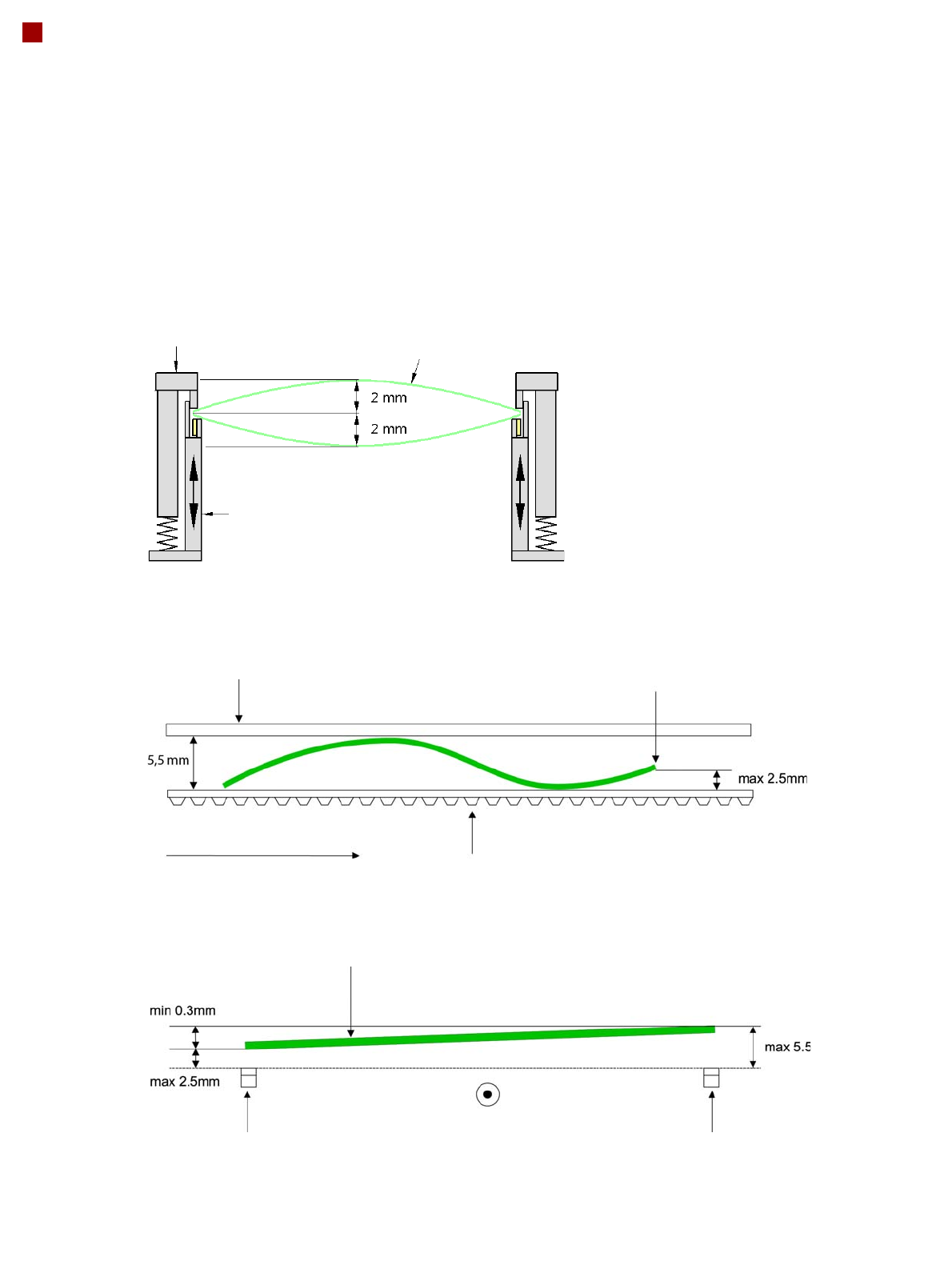
24 PCB Warpage PCB warpage across the direction of travel max. 1 % of the PCB diagonal, but no t exceeding 2 mm PCB warpage during transportation Fixed clamped edge Movable clamping device PCB Fixed clamped ed ge Conveyo…
23
PCB Conveyor
Flexible Dual Conveyor
Technical Data for the Dual Conveyor
Stationary conveyor side Right or left
PCB dimensions
Standard (length x width)
"Long Board with stepping" option
Dual conveyor in "single conveyor" mode
Standard
"Long Board with stepping" option
50 mm x 50 mm to 450 mm x 216 mm
a
50 mm x 80 mm to 850 mm x 216 mm
50 mm x 50 mm to 450 mm x 450 mm
50 mm x 80 mm to 850 mm
a
x 450 mm
PCB thickness
Standard
0.3 mm to 4.5 mm (± 0.2 mm)
(Standard, thicker on request)
Vacuum accessories on request
Thin boards on carrier
PCB Warpage See page 24
PCB weight
b
Max. 3 kg
Clearance on PCB underside
Standard
Option
25 mm ± 0.2 mm
Max. 40 mm ± 0.2 mm
PCB conveyor height 900 mm ± 15 mm (option)
930 mm ± 15 mm (standard)
950 mm ± 15 mm (SMEMA option)
Type of interface SMEMA / Siemens
Component-free PCB handling edge 3 mm
PCB changeover time < 2.5 s
PCB positioning accuracy ± 0.5 mm
Conveyor mode Synchronous or asynchronous
Components on each conveyor Same or different
PCB width on each conveyor Same or different
Inkspot detection on the PCB Synchronous: Possible (no global inkspot)
Asynchronous: Possible
Virtual ink spot handler Optional
Automatic width adjustment Synchronous: Possible
Asynchronous: Possible
a) 850 mm on request
b) Higher weight on request.
24
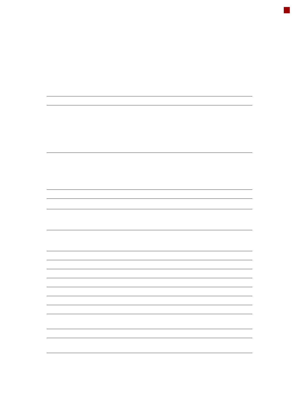
PCB Warpage
PCB warpage across the direction of travel
max. 1 % of the PCB diagonal, but not
exceeding 2 mm
PCB warpage during transportation
Fixed clamped edge
Movable clamping device
PCB
Fixed clamped edge
Conveyor belt
PCB transport direction
Front board edge
Front board edge
PCB warpage in direction of travel + PCB thickness < 5.5 mm
Bending up of front board edge max. 2.5 mm
Left conveyor belt
Right conveyor belt
PCB transport direction
25
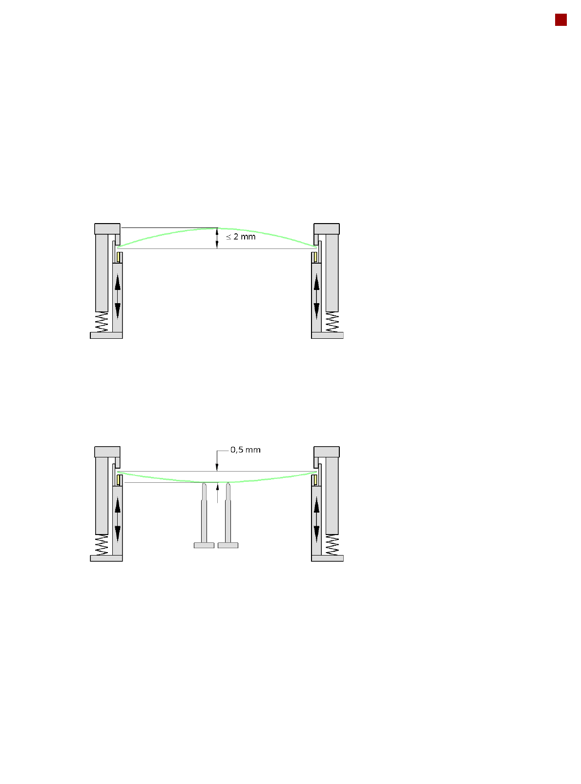
PCB Warpage
PCB warpage during placement
PCB warpage downwards, max. 0.5 mm
Use magnetic pin supports to achieve this
value.
When there is warpage under 2 mm, the
inkspots in the center of the board are also
within the focus of the digital camera. When
all the tolerances are taken into account,
this value is reduced to 1.5 mm.
You should also note that the warpage also
reduces the component height.
Magnetic pin support