IPC-7721(S).pdf - 第133页
OUTLINE This method is used to replate edge contacts by selective swab plating. Edge con- tacts may require replating if they become contaminated with solder or are scratched during handling. Other applications may arise…

NOTES
IPC-7721
Number: 4.6.2
Revision:
Date: 2/98
Subject: Edge Contact Repair, Film Adhesive Method
Page4of4
OUTLINE
This method is used to replate edge contacts by selective swab plating. Edge con-
tacts may require replating if they become contaminated with solder or are scratched
during handling. Other applications may arise when the plating on the edge contacts
does not meet the minimum thickness specification or if the specification changes.
This electroplating process uses a DC power supply. One lead is connected to the
connector edge contacts that need plating. A second lead is connected to the plat-
ing probe. The plating probe has an anode fastened to the tip. The anode has
absorbent wrapping. The anode is dipped into high-speed proprietary plating solu-
tions. When the saturated anode is swabbed across the printed wiring board con-
nector edge contacts, the metal contained in the solution is plated wherever electri-
cal contact is made. Prior to replating any solder contamination must be removed.
CAUTION
This method can be used to replate any metal surface including connector edge
contacts, but it is essential that the surface to be plated is free of deep scratches,
nicks, pin holes or other defects. If the edge contacts need to be replaced see
appropriate procedure.
SAFETY
A thorough review of this method should be made before repairs are attempted.
Technicians should become familiar with the tools included and should practice on
scrap printed wiring boards
To expect the best results a clean work environment is essential. A smooth work
surface and good lighting are recommended. Safety glasses and safety gloves
should always be worn when handling hazardous chemicals.
The work area should be adequately ventilated. It is particularly important to have
adequate ventilation when using gold solution, since gold solution contains a very
small percentage of free cyanide. If ventilation is not adequate, use a fan to move
fumes away from the operator.
CAUTION
It is essential to follow the manufacturer’s instructions supplied with the plating equip-
ment.
REFERENCES
2.1 Handling Electronic Assemblies
2.2 Cleaning
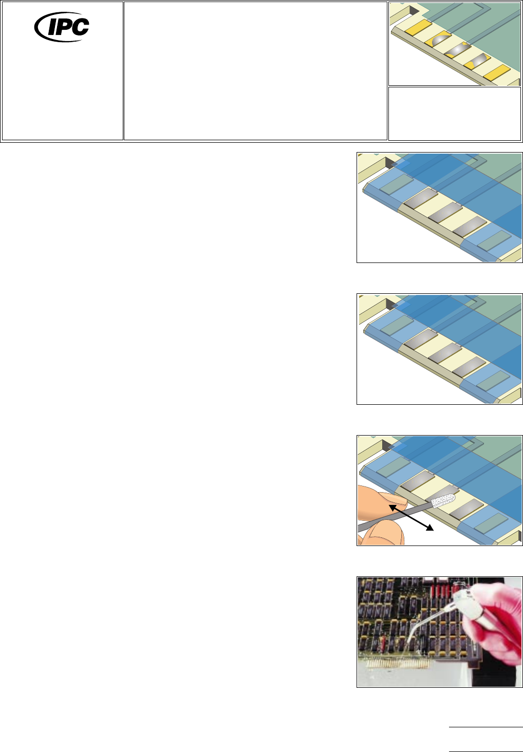
Figure 1 Apply tape.
Figure 2 Flow solder.
Figure 3 Solder stripping solution.
Figure 4 Rinse.
7721
Repair and
Modification of
Printed Boards and
Electronic Assemblies
Revision:
Date: 2/98
Edge Contact Repair,
Plating Method
Number: 4.6.3
Product Class: R, F, W, C
Skill Level: Advanced
Level of Conformance: High
Material in this manual was voluntarily established by Technical Committees of the IPC. This material is advisory only and its
use or adaptation is entirely voluntary. IPC disclaims all liability of any kind as to the use, application, or adaptation of this
material. Users are also wholly responsible for protecting themselves against all claims or liabilities for patent infringement.
Equipment referenced is for the convenience of the user and does not imply endorsement by the ipc.
Page1of6
TOOLS & MATERIALS
Abrasive Pad
Board Support
Burnisher
Cleaner
Cleaner Wipes
Connector Edge
Plating System
Conductive Pen
Desoldering Braid or
Desoldering System
Eraser Stick
Gloves, Antistatic
Polyimide Tape
Knife
Liquid Flux
Peel Testing Tape
Pin Fixtures
Plating Anodes
Plating Cables
Plating Probe
Plating Solution, Gold
Plating Solution, Nickel
Plating Solution, Electroclean
Plating Solution, Solder Strip
Plating Tape
Power Supply
Probe Clip
Rinse Bottle
Rinse Tray
Safety Glasses
Solder
Solder Iron
Solution Cups
Solution Tray
Swab
Thickness Measuring System,
Gold and Nickel
Water/Air Sprayer
Wire, Buss, 30 AWG
Work Sink
PREPARATION − Remove Solder Contamination
CAUTION
Safety glasses and safety gloves should always be worn when handling hazardous
chemicals. Do not work within a small enclosed room without supplemental ventila-
tion. If ventilation is not adequate, use a fan to move fumes away from the operator.
1. Clean the rework area.
2. Apply plating tape to the printed wiring board surface surrounding the area to be
reworked. (See Figure 1.) The plating tape will protect adjacent components and
the printed wiring board surface from unwanted exposure to stripping and plating
solutions.
3. Flow solder over the entire area of any contacts that have contamination using a
soldering iron. This provides a more even surface when plating. Remove the bulk
of the solder contamination using desoldering tools or desoldering braid. (See
Figure 2.)
4. Clean the area.
5. Place the printed wiring board on the board support so that the leading edge
overhangs the rinse tray.
6. Swab the solder stripping solution over the solder contamination using a swab.
Swab the surface until all remaining solder has been stripped off. (See Figure 3.)
7. Thoroughly rinse the entire area with water. (See Figure 4.)
8. Mildly buff the contacts using abrasive pad. Mild buffing will prepare the surface
for plating and remove any remaining solder contamination.
9. Thoroughly rinse with water to remove any residue.
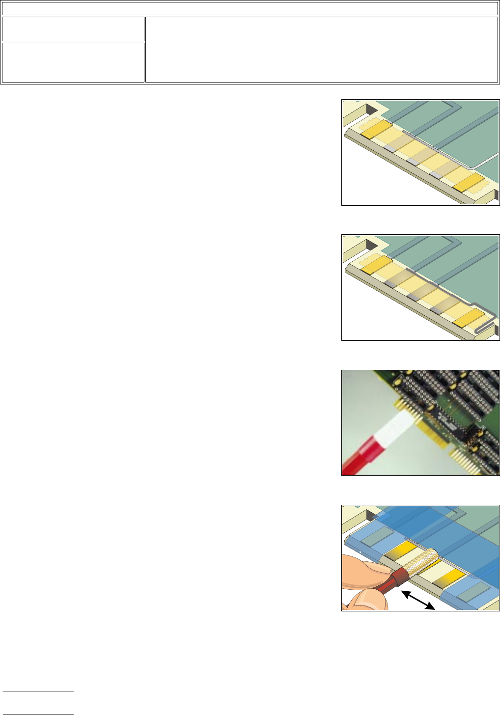
Figure 5 Solder a wire to the edge of
the contacts needing plating.
Figure 6 Apply conductive paint to
the edge of the contacts.
Figure 7 Sample plating anodes
shown with fabric wrapping.
Figure 8 Brush the surface with the
saturated plating probe.
IPC-7721
Number: 4.6.3
Revision:
Date: 2/98
Subject: Edge Contact Repair, Plating Method
Page2of6