Specification SIPLACE CA-Series2011版.pdf - 第40页
40 Vision Sensor Technology PCB Position Recognition Technical data PCB fiducials Local fiducials Library memory f. recognition of bad panel s up to 3 (subpane ls and multiple p an- els) up to 6 for the Long board option…

39
Component supply
SIPLACE Wafer System
Technical data
Electrical values
Noise emissions
Permissible environmental
impact
Supply voltage 3 x 400 VAC, 50 Hz (Europe)
3 x 208 VAC, 60 Hz (USA)
Total output 1.5 kW
Nominal current 2.7 A at 3 x 400 VAC
4.2 A at 3 x 208 VAC
Fuse 3 x 16 A
Nominal current consumption of largest consumer 2 A
Maximum noise emissions 74 dB (A)
Room temperature between 15 °C and 35 °C
Atmospheric humidity 30 - 75 %
(No higher than 45% on average to prevent any
possibility of condensation on the machine)
40
Vision Sensor Technology
PCB Position Recognition
Technical data
PCB fiducials
Local fiducials
Library memory f.
recognition of bad
panels
up to 3 (subpanels and multiple pan-
els)
up to 6 for the Long board option
(Optional PCB fiducials are output by
the optimization.)
up to 2 per PCB (may be of different
type)
up to 255 fiducial types per subpanel
Image analysis Edge detection method (singular fea-
ture) based on grayscale values
Lighting method Front lighting
Fiducial recognition
time
0.1 s
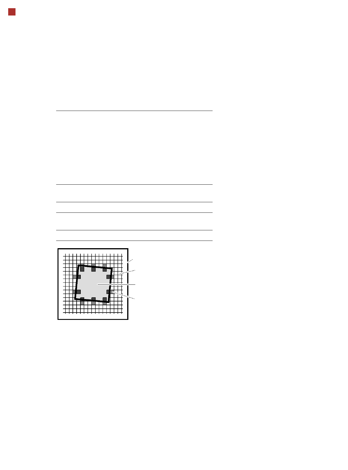
Field of vision 5.78 x 5.78 mm
Camera's field of view
Pixel
Ink spot, e.g. square
Evaluation window
Singular Feature
Description
SIPLACE has a number of
vision modules and a central
vision system to evaluate the
recorded image data, ensur-
ing high placement accuracy.
The PCB vision module is
mounted on the machine's X
gantry. It is used to find the
PCB's positioning-offsets
within the conveyor system.
This vision module is also re-
quired to measure the ma-
chine origin and/or the feeder
module positions on one side
of the table.
Each vision module consists
of a single CCD camera with
integrated lighting and
optics. The offsets in the po-
sition of the PCBs are deter-
mined with the help of at
least two but generally three
reference fiducials on the
PCB. When the PCB arrives
at the placement area the po-
sitioning system with its PCB
vision module moves to the
programmed fiducial. The
edge detection method
allows you to choose pre-
defined fiducials from a
menu (e.g. cross, circle,
square).
The size of the fiducial is pro-
grammed at the station com-
puter. From this time on form
and size of the fiducial is de-
fined and known.
With this data the PCB vision
module is able to search and
recognize the fiducial at the
predefined position on the
PCB or ceramic substrate
without further assistance.
For this reason it places sev-
eral small evaluation win-
dows at the assumed border
of the fiducial. Within these
evaluation windows the vi-
sion system looks for con-
trast transitions between
bright and dark. After finding
such contrasts the actual
position of the fiducial can be
assigned by comparison with
the predefined - and thus
known - shape and size.
The analysis operations can
be used to determine any off-
set with respect to the de-
sired position in the X and Y
directions and the angular
position. Alternatively, a fidu-
cial may be taught as a pat-
tern.
Additional functions of the
PCB vision module include
recognition of the position of
the feeder modules and ce-
ramic substrate (optional)
and recording of the machine
data including mapping.
The bad board detector
(GOOD/SCRAP scan) is also
moved over the ink spot us-
ing the PCB vision module.

41
Vision Sensor Technology
PCB Position Recognition
Description
Different fiducial shapes
prove to be optimal depend-
ing on the condition of the
surface. Particularly advis-
able for bare copper surfaces
with little oxidation is the sin-
gle cross. Maximum accura-
cy is achieved due to the high
information content.
Rectangle, square and circle
are less "informative" but
save space and can even be
used when oxidation is at an
advanced stage.
Advisable for tinned struc-
tures are circle or square be-
cause in this case the ratio of
the fiducial dimensions to the
presolder thickness is partic-
ularly favorable.
Fiducial criteria
Locate 2 fiducials
Locate 3 fiducials
X-/Y-position, rotation angle, mean PCB distortion
Additional: shearing, distortion separately in X and Y direc-
tion
Fiducial shapes Synthetic fiducials: circle, cross, square, rectangle, diamond,
circular, square and rectangular contours, double cross
pattern: any
Fiducial surface:
copper
tin
Without oxidation and solder resist
Warpage 1/10 of structure width, good contrast to sur-
rounding area in each case
Dimensions of synthetical fiducials (standard)
Min. X/Y size for circle and rectangle: 0.25 mm
Min. X/Y size for annulus and rectangle: 0.3 mm
Min. X/Y size for cross: 0.3 mm
Min. X/Y size for double-cross: 0.5 mm
Min. X/Y size for rhombus: 0.35 mm
Min. frame width for annulus and rectangle: 0.1 mm
Min. bar width / bar distance for cross, double-cross: 0.1 mm
Max. X/Y size for all fiducial shapes: 3 mm
Max. bar width for cross, double-cross: 1.5 mm
Min. tolerances, general: 2% of nominal dimension
Max. tolerances, general: 20% of nominal dimension
Dimensions of patterns
min. size
max. size
0.5 mm
3 mm
Fiducial environment Clearance around reference fiducial not necessary if there is
no similar fiducial structure in the search area