forte_en.pdf - 第17页
Page 17 Table of Connections P i n A V R A V R T P I A T x m e g a P D I 8 0 5 1 P R E S E T R E S E T R E S E T - V D D V C C V C C V C C V C C G N D G N D G N D G N D G N D D M O S I T P I D A T A P D I _ D A T A M O S…
Page 16
2.6.2 Programming in ZIF
Socket
If programming of autonomous device is required, i.e.
those that are only later connected to an application, it is
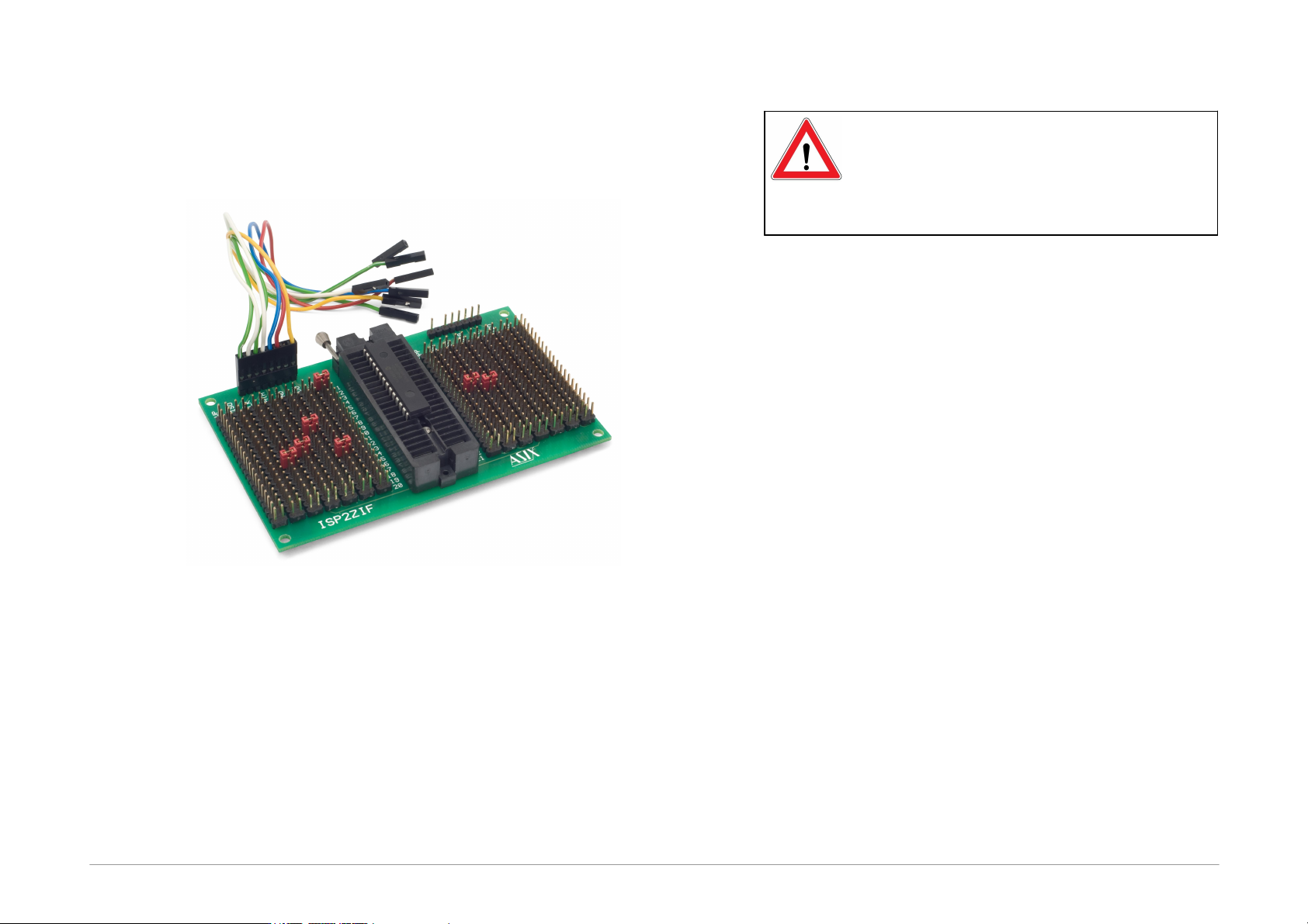
possible by means of our optional ISP2ZIF accessory.
Fig.6: ISP2ZIF
ISP2ZIF consists of a zero insertion force (=ZIF) socket
and an ICSP connector for connecting to the programmer,
which can also provide voltage for feeding the program
circuitry.
2.6.3 Connecting
Procedure
The correct procedure for connecting the programmer:
first connect FORTE to the target application, then
connect FORTE to the USB and finally turn on the
application’s power supply.
Please make sure that the GND of the application, the
programmer and the USB are interconnected before
signals and the power are applied.
Important warning
If an application is powered by a switched
power source or is not grounded, a significant
voltage difference may appear between the
programmer’s ground and the application’s
ground. This could damage the programmer.
The simplest way of connecting the GND prior to the
other signals is to ground the application before
connecting it to the programmer. This can, for example,
be achieved by making the GND pin of the application’s
ICSP connector longer than the other pins. It will make
sure that both grounds are interconnected first.
Page 17
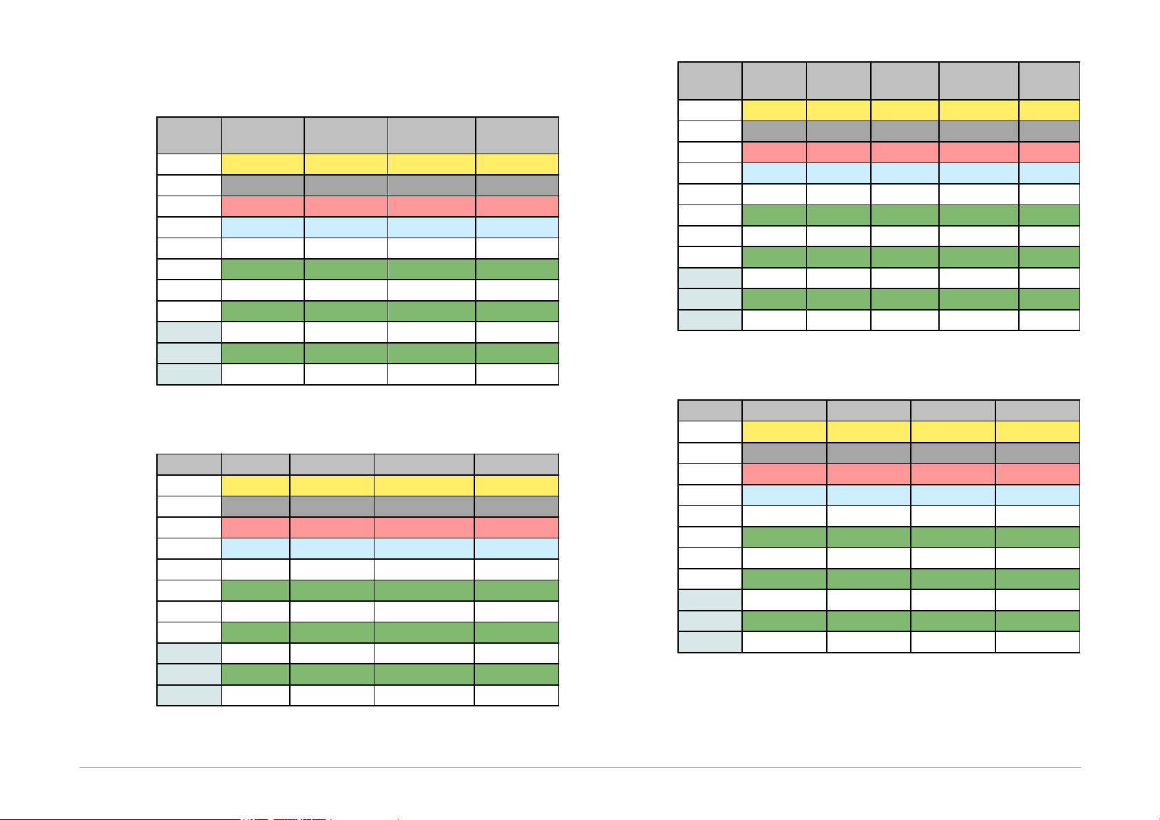
Table of Connections
Pin
AVR
AVR TPI
ATxmega
PDI
8051
P
RESET
RESET
RESET
-
VDD
VCC
VCC
VCC
VCC
GND
GND
GND
GND
GND
D
MOSI
TPIDATA
PDI_DATA
MOSI
C
SCK
TPICLK
PDI_CLK
SCK
I
MISO
MISO
L
SS
T
S
R
Table3: Connection list No.1
Pin
PIC
MSP430
MSP430 SBW
TI CCxxxx
P
MCLR
TEST/VPP
VPP
RESET
-
VDD
VDD
VCC
VCC
VDD
GND
VSS
VSS
VSS
GND
D
PGD
TDI
SBWTDIO
Debug_data
C
PGC
TCK
SBWTCK
Debug_clock
I
TDO
L
LVP
TMS
T
S
R
RESET
Table4: Connection list No.2
Pin
I
2
C
SPI
QUAD
SPI
1
Microwire
UNI/O
P
- CS
- CS
CS
-
VDD
VDD
VDD
VDD
VDD
VCC
GND
GND
GND
GND
GND
VSS
D
SDA
SI
SIO0
DI
SCIO
C
SCL
SCK
SCK
CLK
I
SO
SIO1
DO
L
SIO2
ORG/(PRE)
T
S
SIO3
R
Table5: Connection list No.3
Pin
PSoC
1-Wire
ARM SWD
LPC UART
P
XRST
IO
2
NRST
RESET
-
VDD
VDD
VDD
VDD
VDD
GND
VSS
GND
GND
VSS
D
ISSP-DATA
SWDIO
RXD
C
ISSP-SCLK
SWCLK
TXD
I
ISP
L
T
S
R
Table6: Connection list No.4
Page 18
Pin
JTAG
HCS08
HCSxxx
C2
P
USR
RESET
-
VDD
VDD
VDD
VDD
VDD
GND
GND
VSS
VSS
GND
D
TDI
BKGD
Data
C2D
C
TCK
Clock
C2CK
I
TDO
L
TMS
T
S
R
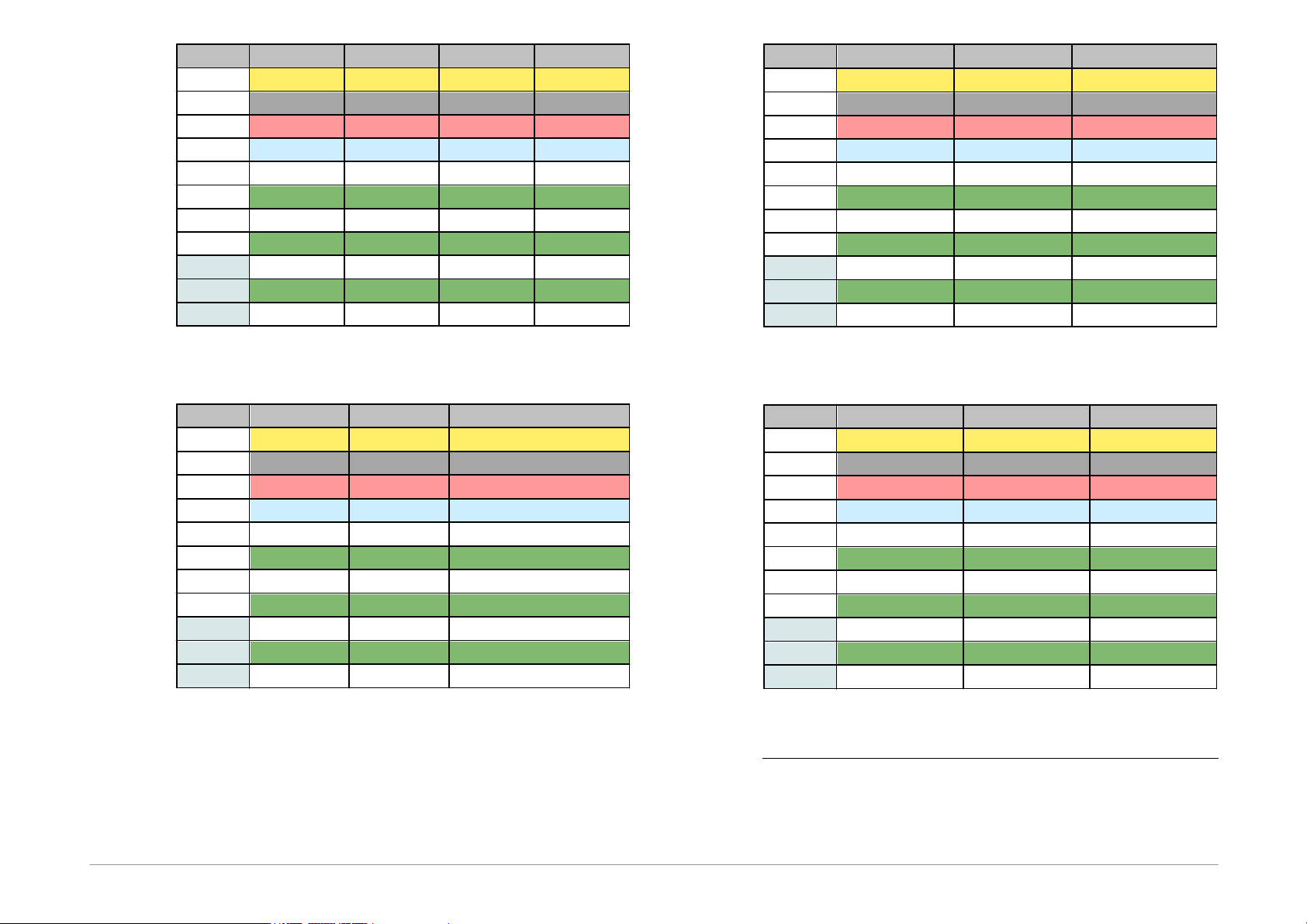
Table7: Connection list No.5
Pin
RL78
RX600
AT89C51CC01UA
P
RESET
RES#
RESET
-
VDD
VDD
VCC
VCC
GND
VSS
VSS
VSS
D
TOOL0
RXD1
RxD
C
TXD1
TxD
I
MD
EA
L
PC7/UB
PSEN
T
S
R
ALE
Table8: Connection list No.6
Pin
AVR HVP
AVR UPDI
3
AVR UPDI+RST
3
P
RESET
UPDI / RESET
RESET
-
VDD
VCC
VDD
VDD
GND
GND
GND
GND
D
SDI
UPDI
C
SDO
I
SII
L
SCI
T
S
R
Table9: Connection list No.7
Pin
CH32V003
SPD5118
Z8F
P
NRST
RESET
-
VDD
VDD
VDDSPD
VDD
GND
VSS
GND
VSS
D
SWIO
HSDA
DBG
C
HSCL
I
L
HSA
T
S
R
Table10: Connection list No.8
1
It is recommended to use a flat ribbon cable and to
connect all its GND wires.