forte_en.pdf - 第29页
Page 29 2) For DS1821: In th ermostat mode, the VDD p in of t he device must be conn ected to the D pin o f t he programmer. However extern al su pply voltage must not be conn ected to th e D pin o f t he programmer. It …
Page 28
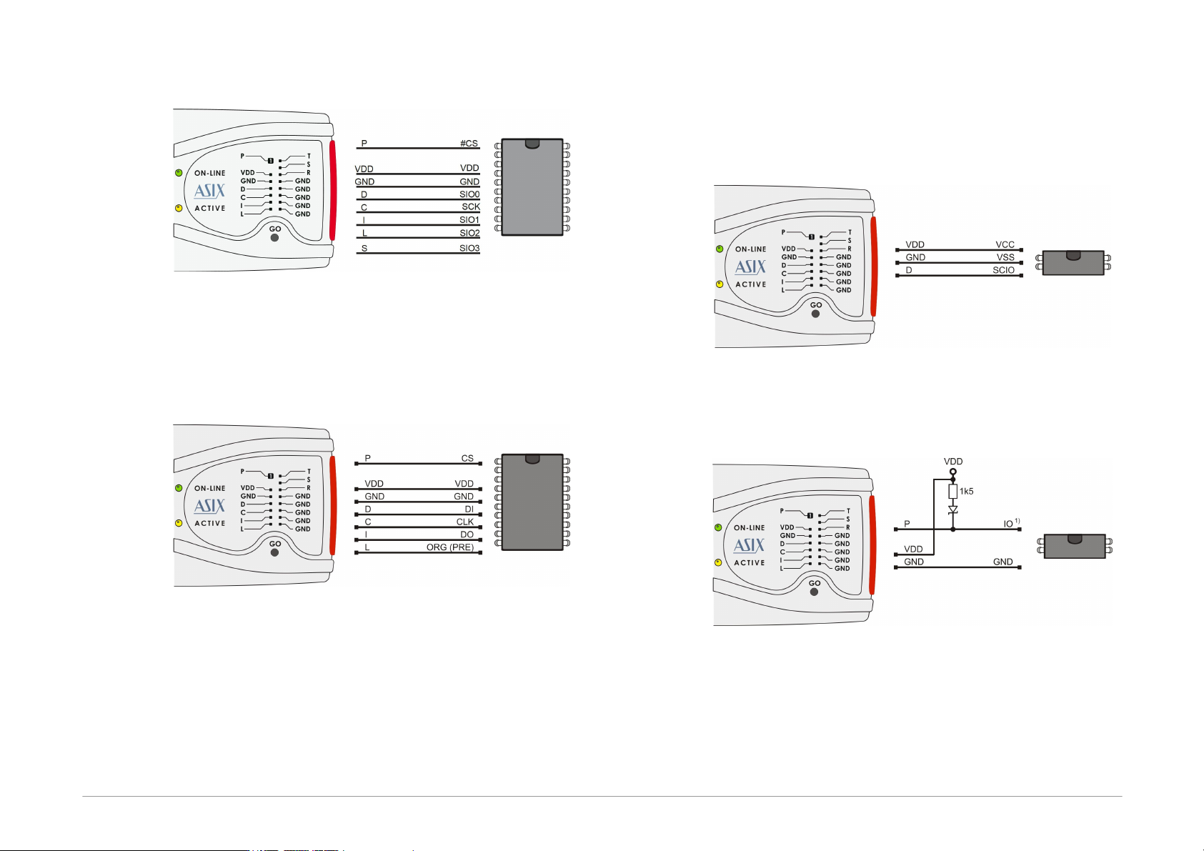
QUAD SPI interface
Fig.32: QUAD SPI interface
1) It is recommended to use a flat ribbon cable and to
connect all its GND wires.
Microwire Memory Chips
Fig.33: Microwire memory chips
1) Pin L determines the memory organization as either
8-bits or 16-bits per word. The user selects the
required organization in the UP program and FORTE
then sets this pin to the corresponding logic level. If
this memory pin is firmly connected to the correct
logic level inside the application, pin L in the
programmer remains disconnected.
2) If used in combination with the M93Sx6 memory chip,
the programmer's L pin must be connected to the
device's PRE pin to serve for selecting the protection
register.
UNI/O Memory Chips
Fig.34: UNI/O serial memory chips
1-Wire Interface
Fig.35: Components with 1-WIRE interface
1) A Schottky diode is necessary only for devices
requiring higher than the power-supply voltage for
programming, such as DS2505 or DS2406, for
example. A pull-up resistor is needed in any case.
Page 29
2) For DS1821: In thermostat mode, the VDD pin of the
device must be connected to the D pin of the
programmer. However external supply voltage must
not be connected to the D pin of the programmer. It
may be connected to VDD pin of the programmer
only. In this case the device must be programmed
standalone!
3) For DS28E05: This device requires lower value of the
pull-up resistor, e.g. 560R.
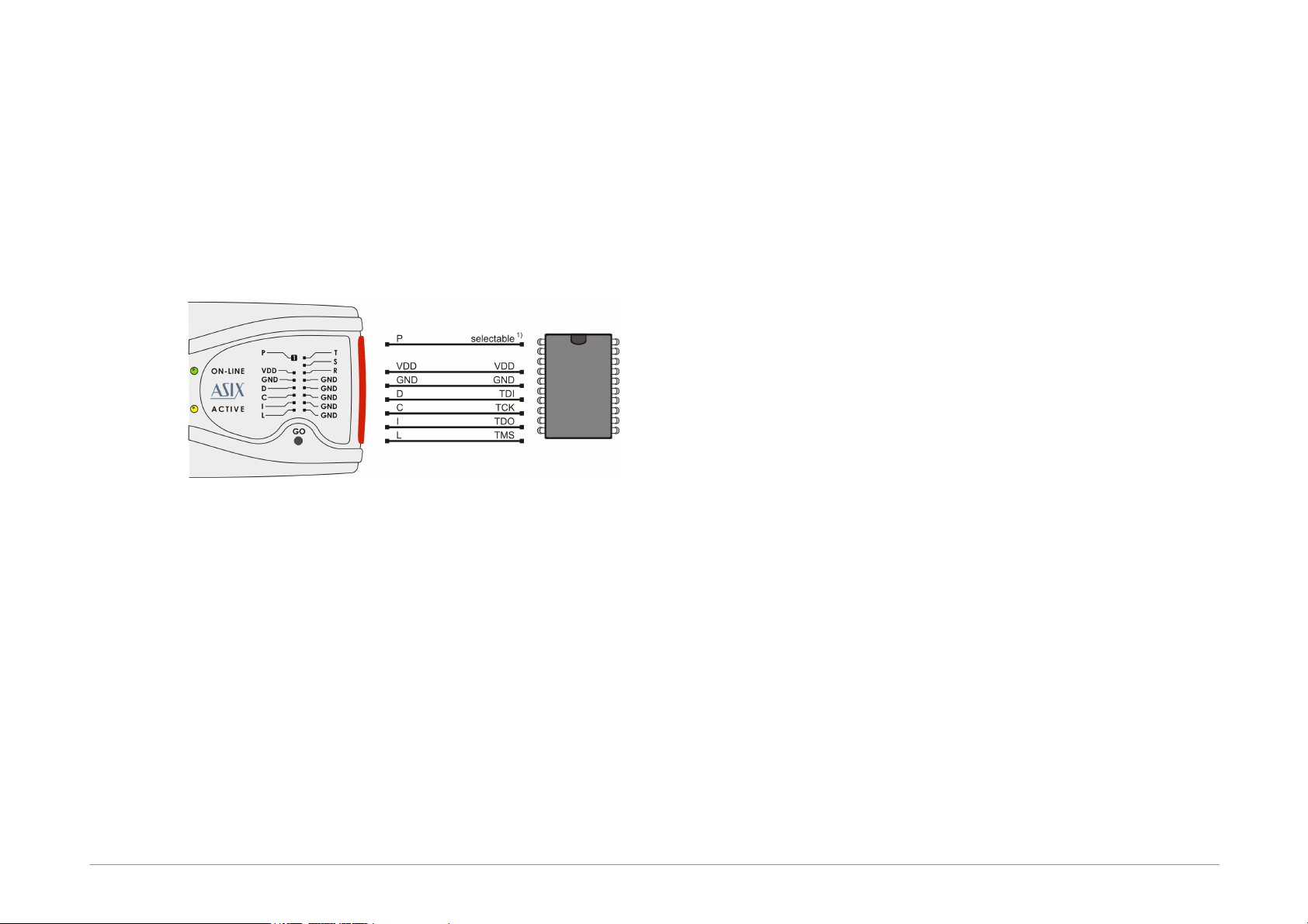
JTAG Interface
Fig.36: Components with JTAG interface
1) Pin P is configurable in the JTAG Player utility. It can
be set to keep the device in reset during
programming. This is needed for ATmega devices, for
example.
2) The programmer always uses an external
power-supply voltage for SVF or XSVF file
programming by means of the JTAG Player
utility.
3) AVR32 microcontrollers are to be programmed from
the UP software through the JTAG interface. The
device must not be reset during programming.
4) ATxmega microcontrollers with the JTAG interface
can be programmed from the UP software through
this interface. Pin P is not needed for programming.
5) ARM microcontrollers can be programmed from the
UP software through the JTAG interface.
a) Devices which have SWD interface, e.g. most of
Cortex-M3 core chips, are programmed via this
interface, see its
connection.
b) Clock source which is connected to the chip and its
frequency must be set in the FORTE programmer
settings window.
c) Using the programmer P pin is not mandatory for
the programming, but it should be connected to the
NRST pin of the device providing reset of the device
after programming to launch the application
program.
d) NXP LPC2xxx: For proper operation, it is required
to tie both /RESET and /TRST pins to FORTE P
output. Further, it is necessary to provide external
pull-down resistor of 4.7kΩ to 10kΩ on the /RTCK
pin. The LPC2xxx MCUs execute on-chip bootloader
after reset. The bootloader then examines pin P0.14
or P2.10 (depends on the part type, see the device
datasheet) to decide whether to start user
application on continue its operation (log.1 for user
application, log.0 for the bootloader). Because of
this, it is necessary to provide an external pull-up
resistor on this pin to start user programmed
application.
Page 30
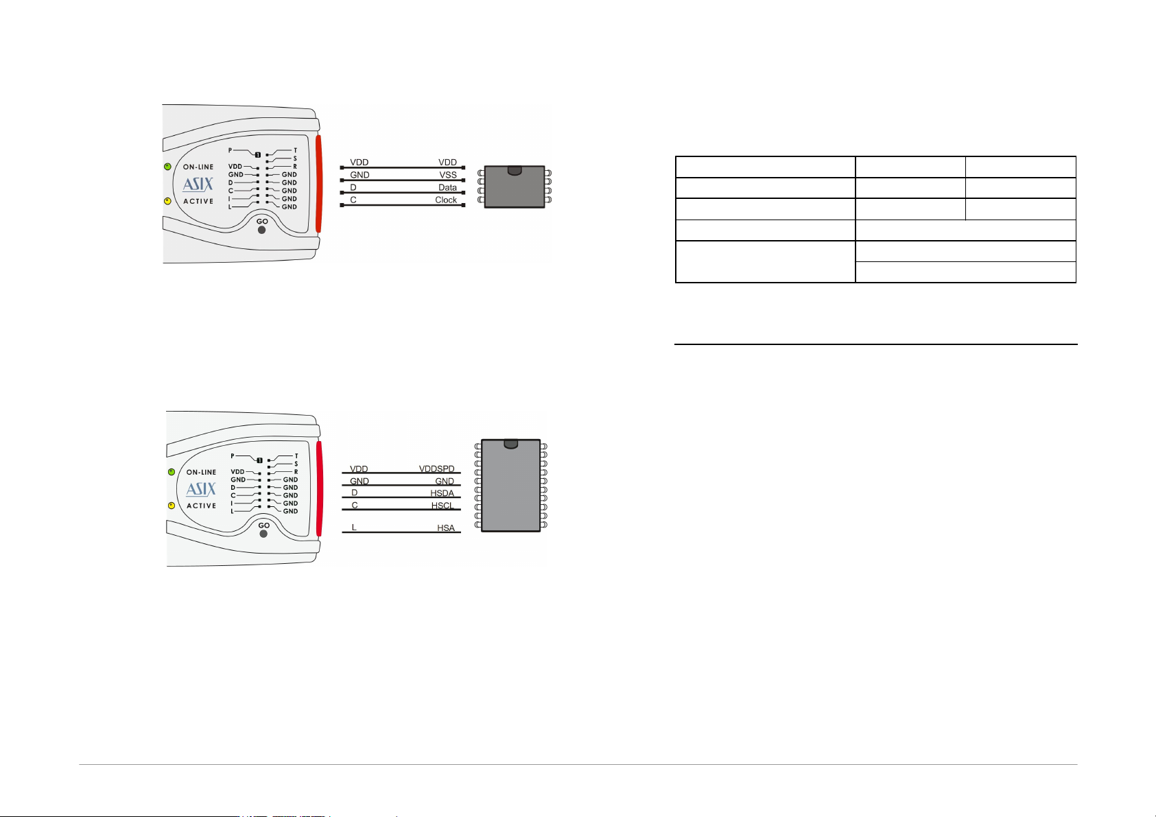
HCSxxx
Fig.37: HCSxxx
1) The Clock signal is usually on S2 pin, the Data signal
is usually on PWM pin.
SPD5118
Fig.38: SPD5118
1) In offline mode an iternal supply voltage from the
programmer has to be used, because a POR with HSA
pin connected to GND is needed. For this mode the
HSA pin of the device can be connected to the L pin
of the programmer. In normal mode the HSA pin do
not have to be connected to the programmer. A write
protection can be disabled in the offline mode only in
registers of MR12, MR13.
2.7
Technical Specifications
2.7.1 Limit Values
Operating temperature
min. 0°C
max. +55°C
Storage temperature
min. -40°C
max. +85°C
Voltage at any pin
1
min. -0.5V
max. 6.5V
Maximum current on I/O pin
50mA
ESD protection (HBM model)
±4kV kontakt
±8kV vzduch
Table12: Limit values
1
Pin P configured as an output has a voltage within a
range of +6.5V to +17V.