forte_en.pdf - 第26页
Page 26 2) Signals used as ISP are listed in the tab le: M i c r o c o n t r o l l e r I S P s i g n a l O t h e r s i g n a l s L P C 1 1 0 2 - - L P C 1 1 x x P I O 0 _ 1 - L P C 1 1 C x x P I O 0 _ 1 P I O 0 _ 3 = L o…
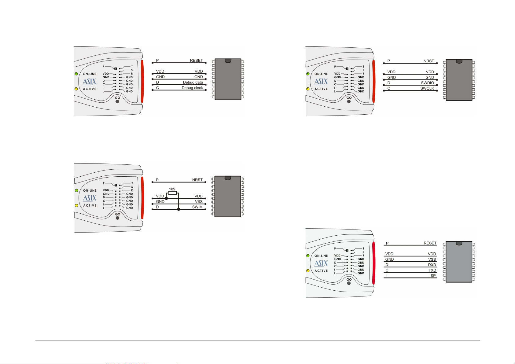
Page 25
TI (Chipcon) CCxxxx
Fig.22: (Chipcon) CCxxxx microcontroller
STM8
Fig.23: STM8 microcontroller
ARM with SWD interface
Fig.24: ARM with SWD interface
1) ARM microcontrollers which do not have SWD
interface are programmed via
JTAG interface.
2) Renesas ARM MCUs with OSIS fuse will lock by
programming of the changed OSIS value. When the
correct OSIS value is filled for a locked MCU, then it is
possible to communicate with the MCU. When the
MCU is erased with the correct value filled, the OSIS
lock will disable.
LPCxxxx, UART interface
Fig.25: LPCxxxx, UART interface
1) UART programming support is implemented for some
LPCxxxx MCUs as an alternative interface to SWD.
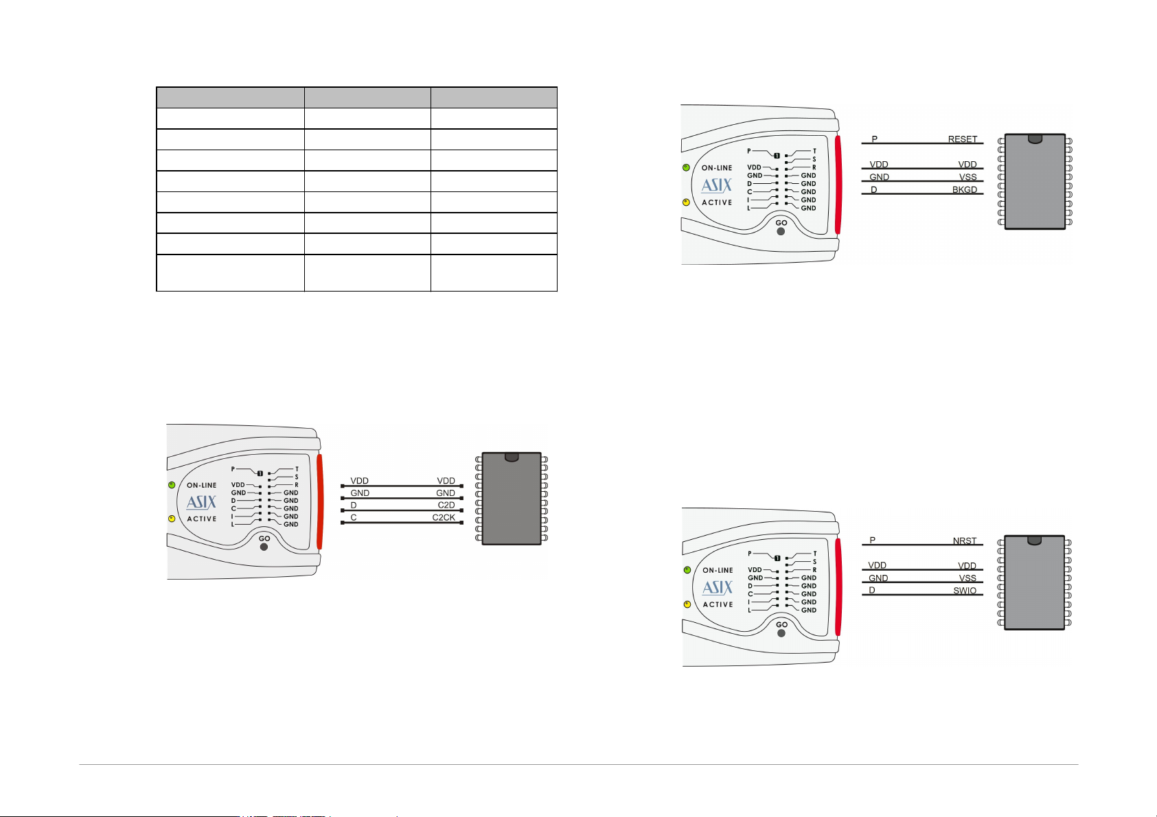
Page 26
2) Signals used as ISP are listed in the table:
Microcontroller
ISP signal
Other signals
LPC1102
-
-
LPC11xx
PIO0_1
-
LPC11Cxx
PIO0_1
PIO0_3 = Log.1
LPC11Uxx, LPC13xx
PIO0_1
PIO0_3 = Log.0
LPC15xx
ISP_0
ISP_1 = Log.0
LPC17xx
P2.10
-
LPC18xx
P2_7
-
LPC5411x
PIO0_31
PIO0_4 = Log.1,
PIO1_6 = Log.0
Table11: ISP signal
C8051 and EFM8 with C2
interface
Fig.26: C8051 and EFM8 with C2 interface
HCS08
Fig.27: HCS08 microcontroller
1) At some devices the programming mode cannot be
entered using their RESET signal, then power-on
reset is used. The programmer cannot do the power-
on reset when UP is controlled using commandline
parameters and external supply voltage is to be
used, in such a case the user have to ensure that the
BKGD pin is in log. 0 during connection of the supply
voltage.
CH32V003
Fig.28: CH32V003 microcontroller
Page 27
Z8F
Fig.29: Z8F microcontroller
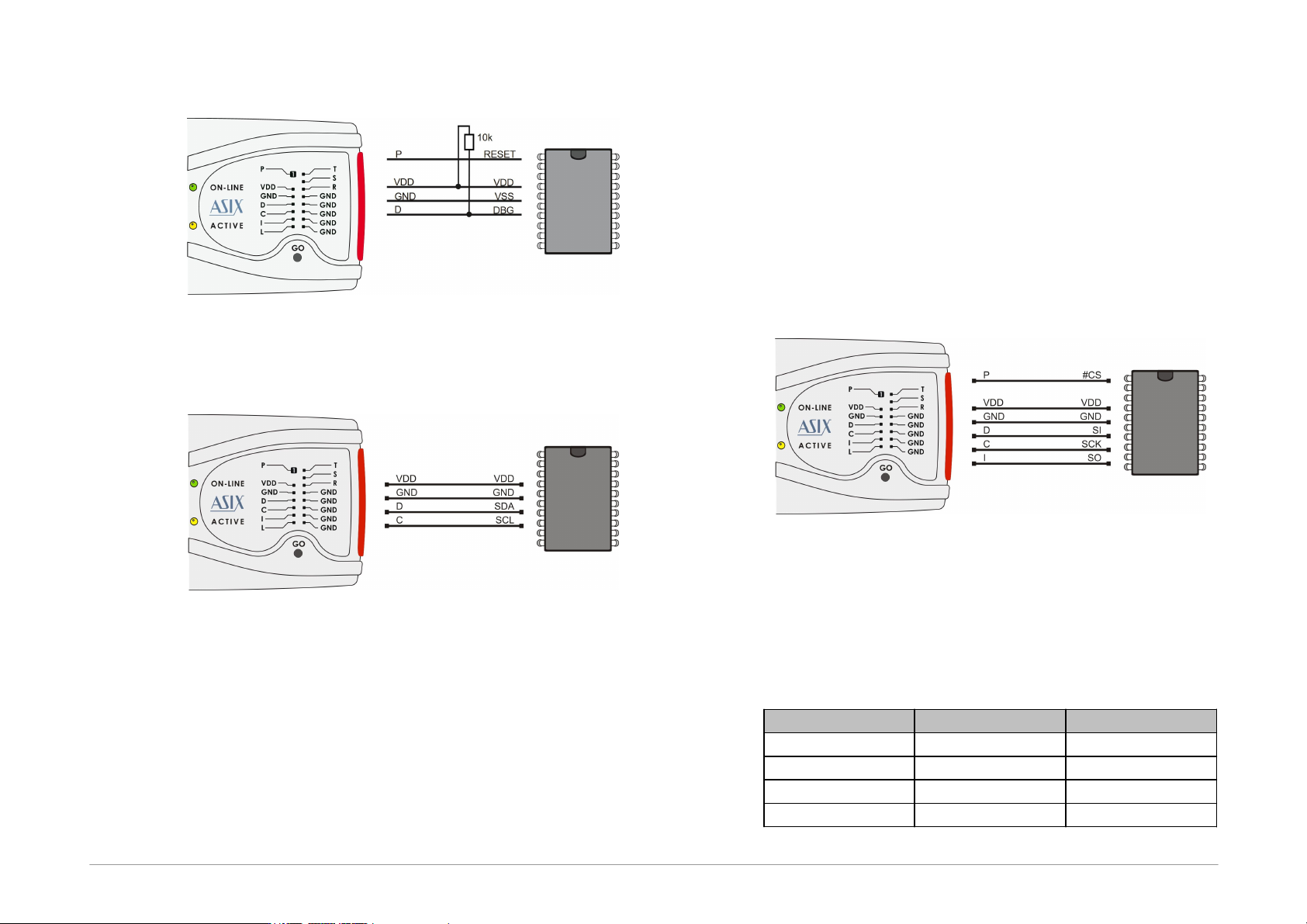
I2C Memory Chips
Fig.30: I2C memory chips
1) The programmer uses an internal 2.2kΩ pull-up
resistor on the data wire (SDA) when working with an
I2C device. This internal resistor can be disabled at
"FORTE programmer settings" window.
2) If the device to be programmed is 24LC(S)21A or
24LC(S)22A, its VCLK pin must be connected to VDD
during programming.
3) 34xx02 memory chips need “high” voltage at the A0
pin for commands protecting it against SWP and
CSWP recording. The “high” voltage is generated at
FORTE P pin, it must be connected to A0 pin in this
case. The memory chip A0, A1 and A2 pins must be
connected manually according to the selected
protection mode.
4) 34AA04 memory needs “high” voltage at the A0 pin
for configuration memory programming. The “high”
voltage is generated at FORTE P pin, it must be
connected to A0 pin in this case.
SPI Memory Chips
Fig.31: SPI memory chips
1) Some devices have WP, HOLD or RESET pins. All of
them must be connected to the required logic level in
such a way as not to block the communication or
device programming.
Different manufacturers mark the memory chips' SPI pins
with different names. Some of them are listed in the
following table:
Name on picture
Atmel, SST
ST
DI
SI
D
DO
SO
Q
CLK
SCK
C
CS
CS, CE
S