forte_en.pdf - 第28页
Page 28 QUAD SPI interface Fig.32: QUAD SPI interface 1) It is rec ommended to use a flat ribbo n cable and to connect all its GND wires. Microwire Memory Chips Fig.33: Microwire memory chips 1) Pin L determines the me…
Page 27
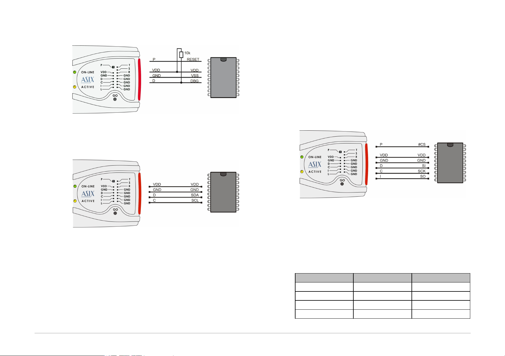
Z8F
Fig.29: Z8F microcontroller
I2C Memory Chips
Fig.30: I2C memory chips
1) The programmer uses an internal 2.2kΩ pull-up
resistor on the data wire (SDA) when working with an
I2C device. This internal resistor can be disabled at
"FORTE programmer settings" window.
2) If the device to be programmed is 24LC(S)21A or
24LC(S)22A, its VCLK pin must be connected to VDD
during programming.
3) 34xx02 memory chips need “high” voltage at the A0
pin for commands protecting it against SWP and
CSWP recording. The “high” voltage is generated at
FORTE P pin, it must be connected to A0 pin in this
case. The memory chip A0, A1 and A2 pins must be
connected manually according to the selected
protection mode.
4) 34AA04 memory needs “high” voltage at the A0 pin
for configuration memory programming. The “high”
voltage is generated at FORTE P pin, it must be
connected to A0 pin in this case.
SPI Memory Chips
Fig.31: SPI memory chips
1) Some devices have WP, HOLD or RESET pins. All of
them must be connected to the required logic level in
such a way as not to block the communication or
device programming.
Different manufacturers mark the memory chips' SPI pins
with different names. Some of them are listed in the
following table:
Name on picture
Atmel, SST
ST
DI
SI
D
DO
SO
Q
CLK
SCK
C
CS
CS, CE
S
Page 28
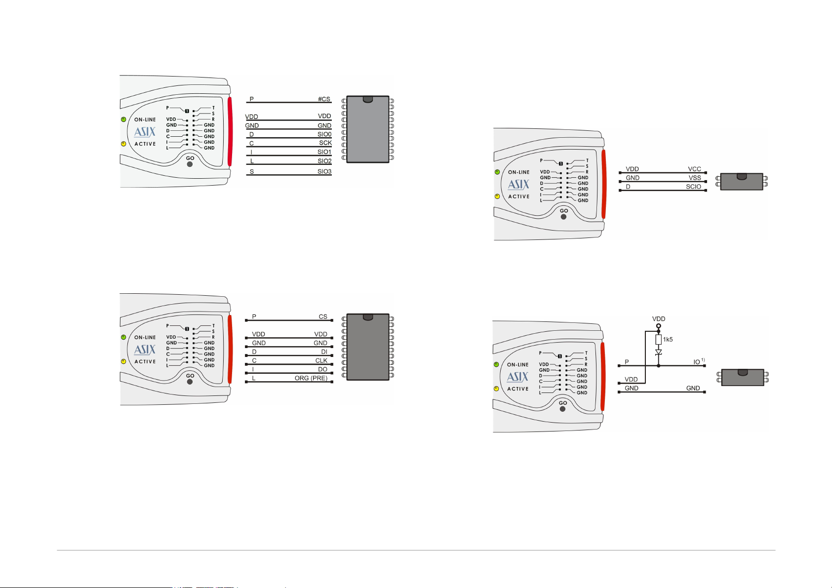
QUAD SPI interface
Fig.32: QUAD SPI interface
1) It is recommended to use a flat ribbon cable and to
connect all its GND wires.
Microwire Memory Chips
Fig.33: Microwire memory chips
1) Pin L determines the memory organization as either
8-bits or 16-bits per word. The user selects the
required organization in the UP program and FORTE
then sets this pin to the corresponding logic level. If
this memory pin is firmly connected to the correct
logic level inside the application, pin L in the
programmer remains disconnected.
2) If used in combination with the M93Sx6 memory chip,
the programmer's L pin must be connected to the
device's PRE pin to serve for selecting the protection
register.
UNI/O Memory Chips
Fig.34: UNI/O serial memory chips
1-Wire Interface
Fig.35: Components with 1-WIRE interface
1) A Schottky diode is necessary only for devices
requiring higher than the power-supply voltage for
programming, such as DS2505 or DS2406, for
example. A pull-up resistor is needed in any case.
Page 29
2) For DS1821: In thermostat mode, the VDD pin of the
device must be connected to the D pin of the
programmer. However external supply voltage must
not be connected to the D pin of the programmer. It
may be connected to VDD pin of the programmer
only. In this case the device must be programmed
standalone!
3) For DS28E05: This device requires lower value of the
pull-up resistor, e.g. 560R.
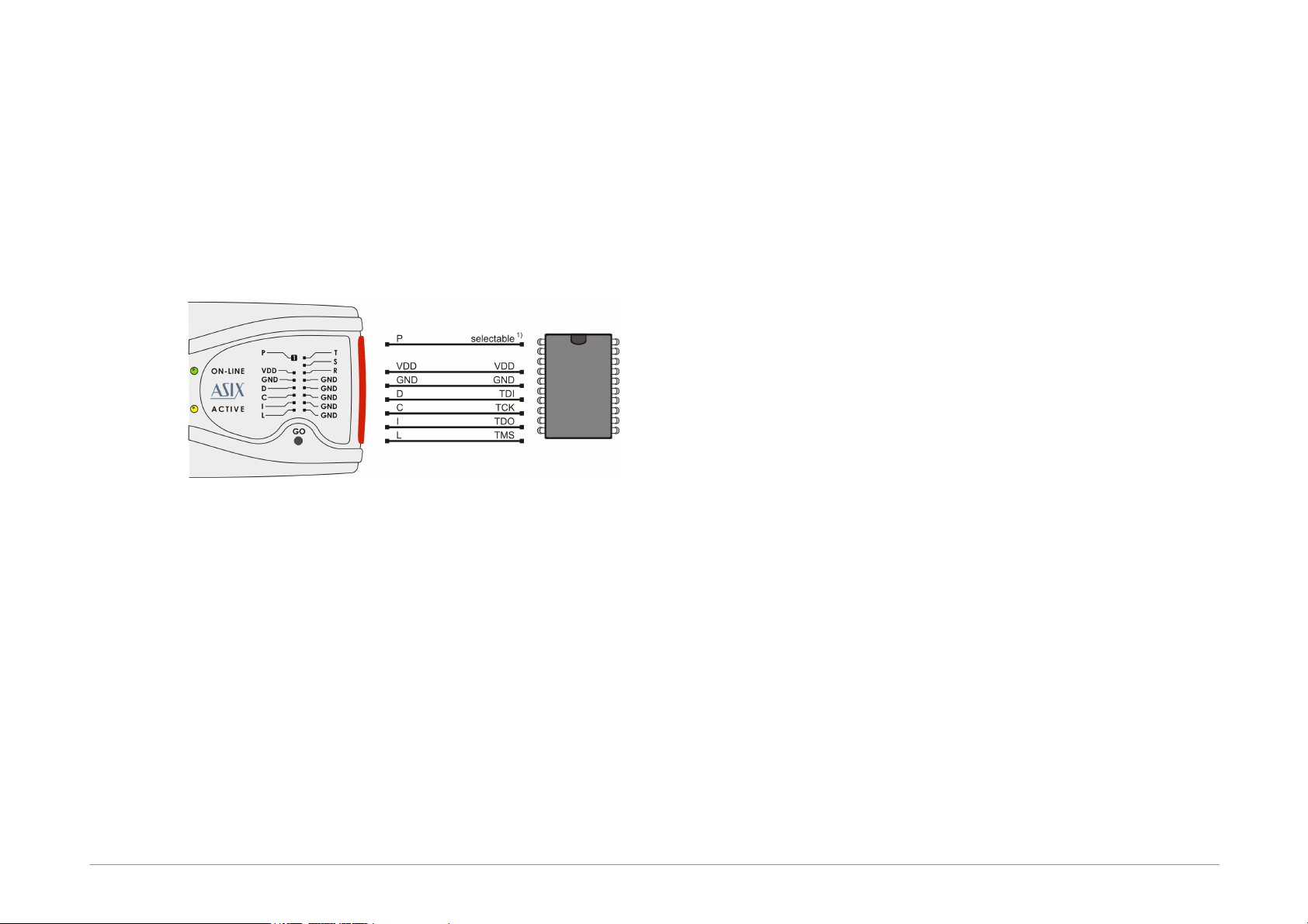
JTAG Interface
Fig.36: Components with JTAG interface
1) Pin P is configurable in the JTAG Player utility. It can
be set to keep the device in reset during
programming. This is needed for ATmega devices, for
example.
2) The programmer always uses an external
power-supply voltage for SVF or XSVF file
programming by means of the JTAG Player
utility.
3) AVR32 microcontrollers are to be programmed from
the UP software through the JTAG interface. The
device must not be reset during programming.
4) ATxmega microcontrollers with the JTAG interface
can be programmed from the UP software through
this interface. Pin P is not needed for programming.
5) ARM microcontrollers can be programmed from the
UP software through the JTAG interface.
a) Devices which have SWD interface, e.g. most of
Cortex-M3 core chips, are programmed via this
interface, see its
connection.
b) Clock source which is connected to the chip and its
frequency must be set in the FORTE programmer
settings window.
c) Using the programmer P pin is not mandatory for
the programming, but it should be connected to the
NRST pin of the device providing reset of the device
after programming to launch the application
program.
d) NXP LPC2xxx: For proper operation, it is required
to tie both /RESET and /TRST pins to FORTE P
output. Further, it is necessary to provide external
pull-down resistor of 4.7kΩ to 10kΩ on the /RTCK
pin. The LPC2xxx MCUs execute on-chip bootloader
after reset. The bootloader then examines pin P0.14
or P2.10 (depends on the part type, see the device
datasheet) to decide whether to start user
application on continue its operation (log.1 for user
application, log.0 for the bootloader). Because of
this, it is necessary to provide an external pull-up
resistor on this pin to start user programmed
application.