prober-english.pdf.pdf - 第17页
■ APPLICATIO NS Wafer ‐ Level Reliability Test Noise Characterization Organic Semiconductor Device Evaluation At the stage of resea rch and development of organic semiconductor device such…
■ APPLICATIONS
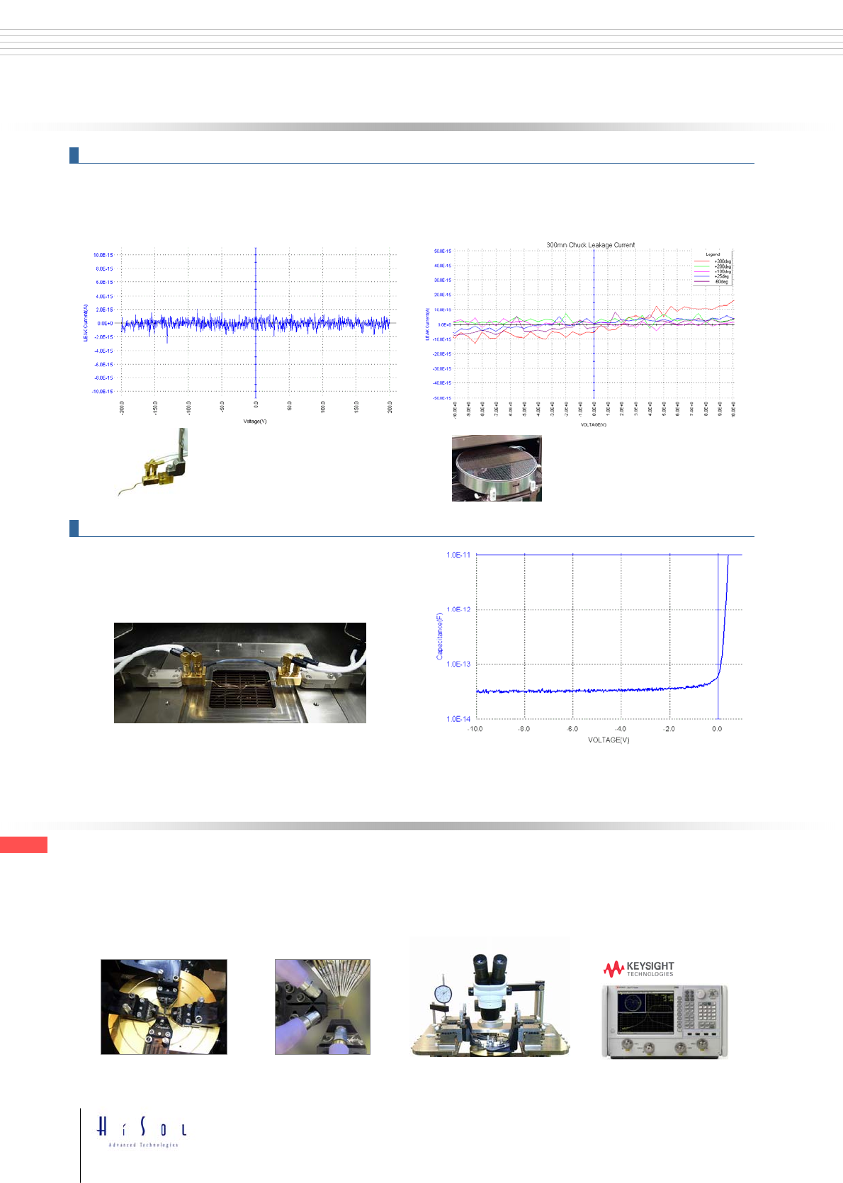
UltraLowSignalI‐V/C‐VMeasurement
High‐frequency/RFmeasurement
Thefollowingplotisaresultofmeasuringthecurrentvaluewhileimpressingthesweepvoltagetotheprobeandthechuckthat are
intheopenstate.Theresultshowsthenoiseandleakcurrentoftheprobeislessthan±10fA.With300mm‐thermalchuck,it
showsthe
noiseandleakcurrentislessthan±20fAinallthetemperatureranges :‐60゜Cto+300゜C.Itprovesthatourprobe
systemcorrespondstoultralowsignalmeasurementapplicationthatrequiresmeasurementprecisionof1pAorless.
Theplotontherightismeasureddataofreversevoltageand
capacitancemeasurementofdiodedevice.
BycorrectingOPEN/SHORT/LOAD, itenablestodostable
C‐Vmeasurementof“fF” level.
C300‐60ULHigh/Lowtemperaturechuck
(‐60゜C~+300゜C)
Voltagesweeprange:‐10V~ +10V
ModelA74CJ1tip‐KelvinCoaxialProbe
Voltagesweeprange: ‐200V~ +200V
Note)Theabovemeasurementvalueisactualmeasurementvalueinourmeasurementenvironmentandnotguaranteedvalue
<±3fA
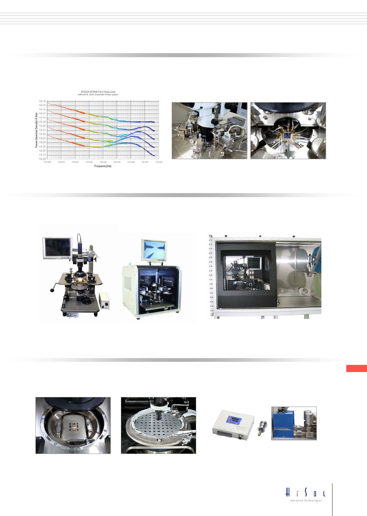
OurprobestationcancovermeasuringfrequencybandofDCto67GHz duetoitshighrigidityandstablemechanism.
SystemintegrationwithVector networkanalyzer(VNA),RF probe,RF cable,calibrationsubstrateetc.,willsupporthighfrequency /
RFmeasurementwhichishighresolutionandexcelsinrepeatability.
Itsupportsfrom2‐porttomulti‐port
measurement,temperaturerangefrom10kto+250゜C,andcharacterizationunderultra‐high
vacuum(10e‐6Pa)environment.
UltralowcurrentI‐Vmeasurement
UltralowcapacitanceC‐Vmeasurement
16
Applications
‐65゜C~+200゜C:<±10fA
+300゜C:<±20fA
■ APPLICATIONS
Wafer‐LevelReliabilityTest
NoiseCharacterization
OrganicSemiconductorDeviceEvaluation
Atthestageofresearchanddevelopment oforganicsemiconductordevicesuchasOFET,OTFT,OEL,andOLED,itisnecessary
toperformevaluationunderhigh‐purityinertgastoavoidcharacteristicdegradationcausedbymoistureoroxygeninthe
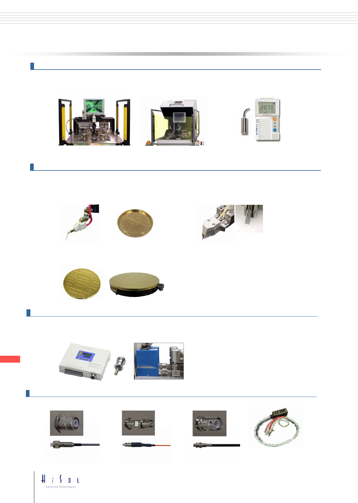
atmosphere.Weoffersmall‐footprintmanualproberandsemi‐autoproberthat
arespeciallydesignedfortheusageinsideofa
glovebox.Theyaresuitableforoperationbyglovedhand.
Manualproberforglovebox
Semi‐automatic proberforglovebox
+300゜CHightemperaturemulti‐siteprobecard
Anoxygenmeterinsideofachamberandamass flow
controller (MFC)enable probingwithalowresidual
oxygenconcentrationoflessthan100ppm
Weofferprobesystemsthatsupportwafer‐levelreliabilitytestsuchasEM,TDDB,HCI,NBTI,BT,etc.,.
Ourprobesystemsupport
varioustasksrequiredinwafer‐levelreliabilitytestsuchashightemperatureupto+300゜C,long‐term
testingoverweeks,stablecontactunderhightemperatureenvironment,mountingmulti‐siteprobecard,anti‐oxidation
environmentbynitrogengaspurge,etc.,.
Ourprobesystemwithshieldchamber (HMP‐810SC/1210SC,HSP‐200SC/300SC)hasoptionsettingofultralowfloornoise(‐UL).
Bychoosingthis“–UL” option,itcansupporton‐wafernoisecharacterizationsuchas1/fnoise,randomtelegraph noise,(RTN),and
RFnoiseinthewidetemperaturerangefrom‐65゜Cto+200゜C.
17
Applications
■ APPLICATIONS
High‐PowerDeviceMeasurement
Safety
HighVoltageMeasurement(~ 10kV),High CurrentMeasurement ( ~ 200Apulse )
Inhigh‐powerdeviceevaluationwheredangeroushighvoltageandhigh currentarerequired,safetymeasuresagainsthumanhaveto
betakeninanticipationofvariouscases.Ourprobesystemfor high‐powerdevicemeasurementisequippedwithinterlocksystemthat
isstandard.Eachinterlocksystemwillpreventfromelectricshock,aburn,
andoxygenshortage
Interlockthatinterruptsappliedhighvoltagewithsafetylight curtain.
Interlockthatpreventsoxygenshortagewith
openairoxygenmonitor.
(Appliedtoasystemwithgaspurgefunction. )
HighVoltageProbing
High CurrentProbing
Weofferprobeaccessoriesthatsupportmaximum10kV200Apulseaswellaschucksthatsupportmaximum 5kV40Apulse.
Itsupportsdevicecharacterizationinthetemperaturerangefrom‐60゜Cto+300゜Cinordertosupportoperationtestinwidetemperature
rangefordevicessuchasin‐vehicledevices.
ChucksforPowerDevices
Highvoltageprobeunit
(±3kV,‐60゜Cto+300゜C)
Insulationliquidimmersiontray
topreventelectricdischarge
High currentprobeunit
(Maximum200Apulse,‐60゜Cto+300゜C)
+300゜CHighTemperatureTest, AntioxidantEnvironment
WhenevaluatingGaN orSiC highpowerdevice,hightemperaturetestat+300゜Cisrequired.Ourproductwithshieldchambermakesit
possibletodonon‐oxidation probingwithalowresidualoxygenconcentrationoflessthan100ppmbypurgingnitrogengasintothe
chamber.
Weofferchuckunitsspeciallydesignedforhighpower
devices.
・ Roomtemperaturechuckandhightemperaturechuck
(RT ~+200゜C/+300゜C),
high/lowtemperaturechuck (‐40゜C/‐60゜C~+200゜C/+300゜C)
・ 5kV 40Apulse
・ Thinwaferhandling
Feed‐throughConnectorsandMeasurementCables
Weoffermeasurementcablesandfeed‐throughconnectorsthatconnectvarioushighpowerdevicetesterswithourprobesystem.
・ Kelvin connection
・ TAIKO processwafer
Keysighttechnologies
B1505A HV‐TRIAX
TFF/KeithleyInstruments
2600‐PCT/4200‐PCT
HV‐TRIAX
SHV connector & cable
(~10kV)
IWATSU
CS‐3000/5000
Itsupportsclosedloopcontrolbyusingoxygenmeterinsideof
achamberandmass flowcontroller(MFC ).
18
Applications