prober-english.pdf.pdf - 第5页
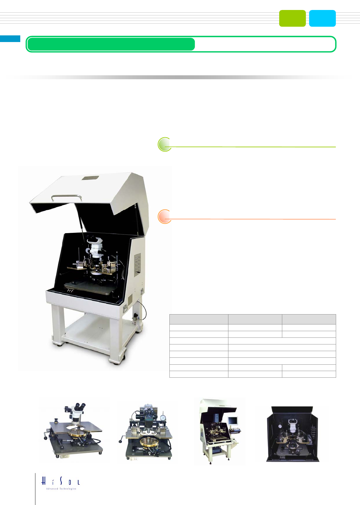
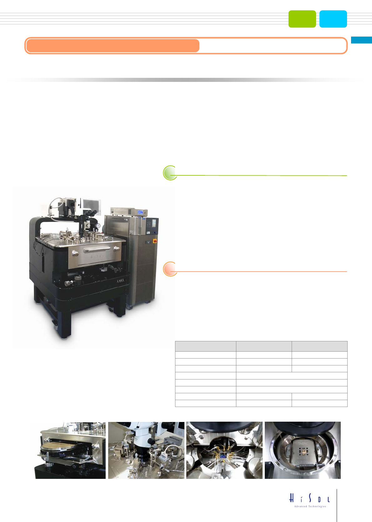
8 inch 12 inch ■ MANUAL PROBER Model HMP-810SC / HMP-1210SC ・ Model HM P-800SC i s for 8" wafers . ・ Model H MP-1200SC i s for 12" wafe rs. Manual Prober for High /L o w Temperature Tests This is …
4
8inch 12inch
Model HMP-800 / HMP-1200
Thisisastandardmanualproberthatsupports8”or12”wafers.
・
Model HMP-800 is for 8" wafers.
・
Model HMP-1200 is for 12" wafers.
Thisprobersupportsreliableon‐wafermeasurementswithasimpleyethigh‐accuracymechanismthatiseasytooperate.
Thisstandardmanualprobermodelisscalabletosupportawiderangeofapplicationssuchashotchucksystems
(fromroomtemperatureto+200°Cor+300°C),submicronresolutionstages,and
lasercutters.
Applications
‐ Temperaturecharacteristicstestsinrangefrom+20°Cto+300°C
‐ UltralowsignalI‐Vmeasurements(fAlevel)
‐ VariousC‐Vmeasurements(quasi‐staticC‐V,HF‐CV,andRF‐CV)
‐ RFmeasurements(upto67GHz)
‐ Ultrahigh‐speedI‐Vmeasurements
Extended applications
‐ Probecardsupport(cansupportMultisiteWLR)
‐ Built‐inlasercutter(Pointmarking,Exfoliationofprotectionlayer,
Metallayercutting)
‐ Probingwithsubmicronaccuracyachievedbyabuilt‐in
metallograph,activevibrationisolator,andultrahigh‐accuracy stage
‐ Light‐receiving/emittingcharacteristicsevaluationapplications
foroptoelectronics (suchasLED,LD,VCSEL,andPD)
‐ Common
gatepad contactsofflat‐paneldisplaydevices
‐ High‐powerdevicemeasurements
(200Apulse,±3kVtriaxial,±10kVcoaxial)
‐ Waferlevelreliabilitytests(suchasEM,TDDB,HCI,NBTI,andBT)
■ MANUAL PROBER
WaferSize
X‐Ycoarsetravel
X‐Yfinetravel
θ travel
PlatenZaxisaction
Unitdimension(W×D×H)*
Weight*
PlatenZaxisadjustment
HMP‐800 HMP‐1200
~φ200mm ~φ300mm
X:205mm,Y:300mm X:305mm,Y:400mm
550×650×450mm
690×780×450mm
60kg 80kg
XY:13mm/Micrometerhead
coarse±30°,fine±2.5°
0/0.3/10mm
0~13mm
*Itemswithasteriskvarydependingonsystemconfiguration.
ManualProber
8inch 12inch
■ MANUAL PROBER
Model HMP-810SC / HMP-1210SC
・
Model HMP-800SC is for 8" wafers.
・
Model HMP-1200SC is for 12" wafers.
ManualProberforHigh/LowTemperatureTests
Thisisamanualprobesystemfornext‐generationsemiconductordevicesdesignedforlownoiseandlowleakage.
Inthissystem,ashieldedchamberstructurecontainstheprobeandchuckinatotallyEMIshieldedenvironment.
Thesystemsupportsmeasurementssuchasultralowsignalmeasurementinthethresholdregions,1/f
noisemeasurement,
Sparameteracquisition,andhigh‐speedI‐Vmeasurementinatemperaturecontrolrangefrom‐60°Cto+300°C
(or+400°Cwhenusingthespecialoption).
Thisprobesystemcanoptionallysupporthigh‐currentandhigh‐voltagepowerdeviceapplications.
*TheHMP‐610SCfor6” wafersisalso
available.
Applications
‐ Temperaturecharacteristicstestsinrangefrom+25°Cto+300°C
orfrom‐60°Cto+300°C
‐ UltralowsignalI‐Vmeasurements(fAlevel)
‐ VariousC‐Vmeasurements
(quasi‐staticC‐V,HF‐CV,andRF‐CV)[subpFlevel]
‐ 1/fnoiseevaluation
‐ RTN(random telegraphnoise)evaluation
‐ High‐frequencynoiseevaluation(upto800MHz)
‐ RFmeasurements(upto67GHz)/Sparameteracquisition
‐ Ultrahigh‐speedI‐Vmeasurements
Extended applications
‐ Probecardsupport(cansupportMultisiteWLR)
‐ Light‐receiving/emittingcharacteristicsevaluationapplications
foroptoelectronics(suchasLED,LD,VCSEL,andPD)
‐ Commongatepad contactsofflat‐paneldisplaydevices
‐ High‐powerdevicemeasurements
(200Apulse,±3kVtriaxial,±10kVcoaxial)*8” model
‐ Waferlevelreliabilitytests
(suchasEM,TDDB,HCI,
NBTI,andBT)
WaferSize
X‐Ycoarsetravel
X‐Yfinetravel
θ travel
PlatenZaxisaction
Unitdimension(W×D×H)*
Weight*
PlatenZaxisadjustment
HMP‐810SC HMP‐1210SC
~φ200mm ~φ300mm
X:205mm,Y:205mm X:310mm,Y:310mm
1020×1000×1550mm
1150×1100×1550mm
750kg 1000kg
±7.5°
0/0.3mm
0~13mm
X:205mm,Y:205mm X:310mm,Y:310mm
*Itemswithasteriskvarydependingonsystemconfiguration.
5
ManualProber
4inch 6inch
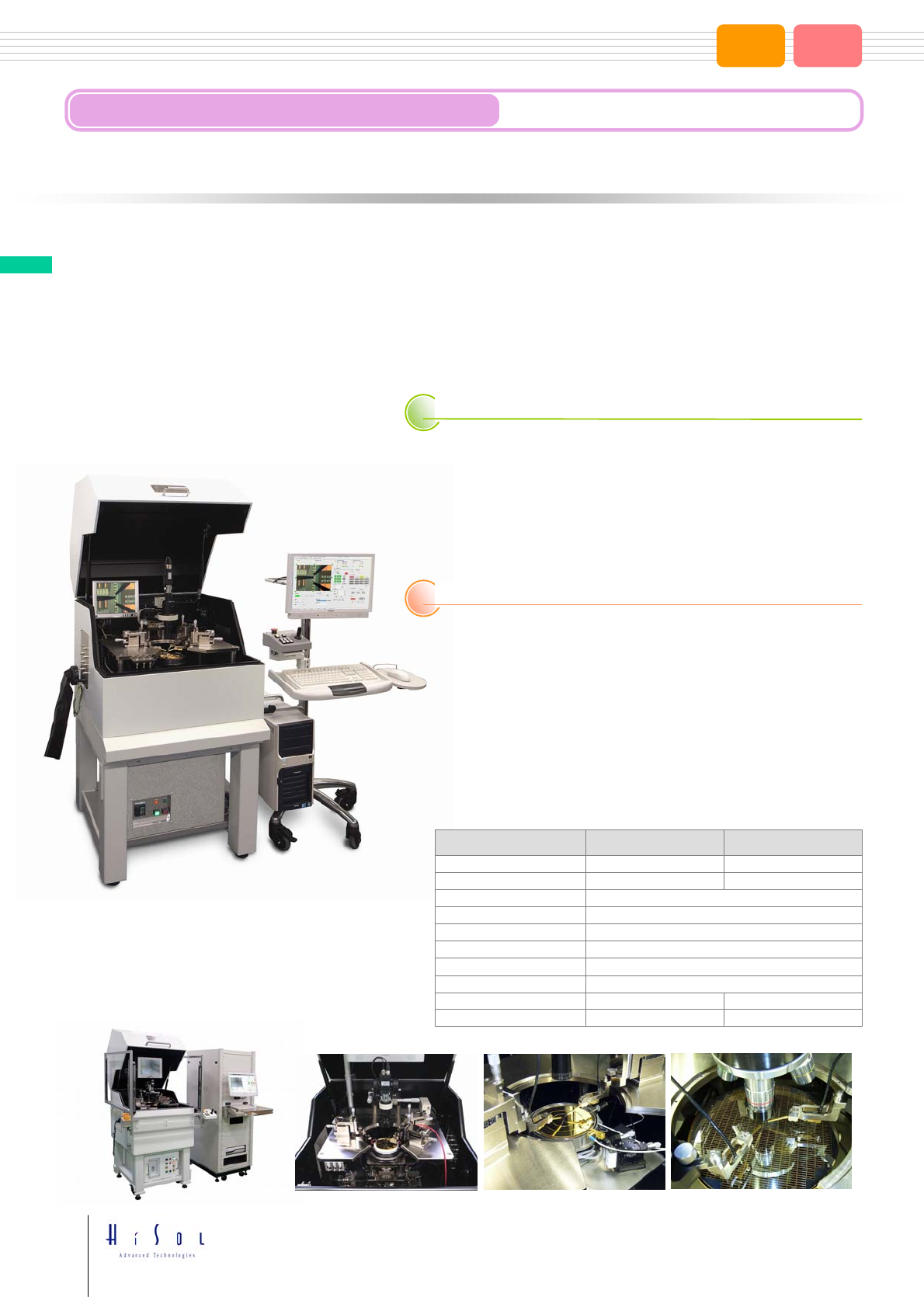
■ SEMI-AUTOMATIC PROBER
・
Model HSP-100 is for 4" wafers.
・
Model HSP-150 is for 6" wafers.
Semi‐AutomaticProbeSystemforSmall‐DiameterWafers
Thisisasemi‐automaticprobesystemthatsupports4” or6” smalldiameterwafers.
Equippedwithahigh‐accuracyX‐Y‐Z‐θ quadraxial closedloopstagehavingexcellentpositioningaccuracyandrepeatability,
thisprobesystemensuresreliableprobecontact.
Thisprobesystemcanincorporateahotchuckthatsupportsatemperaturerangefrom
+20°Cto+300°C.
Thisprobesystemcanoptionallysupporthigh‐currentandhigh‐voltagepowerdeviceapplications.
Applications
Extended applications
‐ Temperaturecharacteristicstestsinrangefrom+20°Cto+300°C
‐ UltralowsignalI‐Vmeasurements(fAlevel)
‐ VariousC‐Vmeasurements(quasi‐staticC‐V,HF‐CV,andRF‐CV)
‐ RFmeasurements(upto67GHz)
‐ Ultrahigh‐speedI‐Vmeasurements
‐ Probecardsupport(cansupportMultisiteWLR)
‐ Built‐inlasercutter
(Pointmarking,Exfoliationofprotectionlayer,Metallayercutting)
‐ Activevibrationisolatorandultrahigh‐accuracyprobingthrough
imageprocessingpatternrecognition(accuracy:± 1umorfiner)
‐ Light‐receiving/emittingcharacteristicsevaluationapplicationsfor
optoelectronics(suchasLED,LD,VCSEL,
andPD)
‐ Commongatepad contactsofflat‐paneldisplaydevices
‐ High‐powerdevicemeasurements
(200Apulse,±3kVtriaxial,±10kVcoaxial)
‐ Waferlevelreliabilitytests(suchasEM,TDDB,HCI,NBTI,and BT)
6
WaferSize
X‐Ytravel
X‐Yrepeatability
X‐Yaccuracy
Ztravel
Unitdimension(W×D×H)*
Weight*
Zrepeatability
HSP‐100 HSP‐150
~φ100mm ~φ150mm
X:105mm,Y:200mm X:160mm,Y:250mm
1200×900×1550mm
1250×900×1550mm
650kg 700kg
<±2μm
<±5μm
20mm
<±1μm
θ travel
θ repeatability
±7.5°
0.002°
*Itemswithasteriskvarydependingonsystemconfiguration.
Model HSP-100 / HSP-150
Semi‐AutomaticProber