SOM-1619-001.pdf - 第11页
11 Tg0590-PM-SO 0301-002 4. PCB Origin Of fset T each (5) Check the setting of T each Point. Press the [TEACH] button *5 and then within two seconds, press the [ENABLE] button on the operation panel. The teaching operati…

10 Tg0590-PM-SO0301-002
4. PCB Origin Offset Teach
*11 Control Switch
When the [ENABLE] button is pressed on the operation panel
within two seconds after the "Move" [ON] button is pressed,
the device is activated.
4.2 PCB Origin Offset Teach Operation Procedure
••
••
• Operation Procedure
(1) Select the [Move to Teach Pt] button *4 and then press the
"Move" [ON] button *11. Then, within two seconds, press the
[ENABLE] button on the operation panel.
The X/Y table will move to the teach point where automatically
judged in the pattern program, the P.E.C. recognition mark or
component outer shape display and land are displayed within the
window size.
(2) Check the view of the P.E.C. recognition mark or component
outer shape display and land displayed within the window size.
(3) When the teach point is the P.E.C. recognition mark, press the
[TEACH] button *5 and then, within two seconds, press the
[ENABLE] button on the operation panel. The P.E.C. recognition
will be performed. When the recognition is completed normally,
the new PCB origin offset (X, Y) is displayed in the teach result
box.
(4) When the teach point is the placement position, select [1-Pt] or
[2-Pt] button in the "Teach Point" box *7.
When the entire component's outer shape is within the
window size:
Select [1-Pt] button (Component Center) for the Teach Point
When the entire component's outer shape is not within the
window size:
Select [2-Pt] button (Opposite Angles in Component) for the
Teach Point. When [2-Pt] button is selected, the PCB pattern
moves to the second point after completing the teaching of first
point.

11 Tg0590-PM-SO0301-002
4. PCB Origin Offset Teach
(5) Check the setting of Teach Point. Press the [TEACH] button *5
and then within two seconds, press the [ENABLE] button on the
operation panel. The teaching operation will be performed.
(6) Manipulate the pointing device to accommodate the component
outer shape image within the window size to the PCB pattern
entered in the recognition memory image.
Operation of Pointing Device
Joy Stick : Movement of the X/Y table (PCB
Pattern)
Right Click : Enlargement of Image
Left Click : Reduction of Image
Click on the Right and Left at the same time
: Positioning Completion
When the positioning is completed, the new PCB origin offset is
displayed in the "Teach Result (X, Y)" box *2.
(7) When the new PCB origin offset is temporarily entered, press the
[Temp Entry] button *3.
The new PCB origin offset is temporarily written in the temporary
file.
(a) Temporarily entering new PCB Origin Offset saves
the temporary file in the data for the operation and
pattern program file, but does not overwrite the
original file.
(b) Cancellation of temporarily entered data is available
during the temporary enter operation. To cancel,
press the [Cancel] button *9.
(8) Check the temporarily entered data using the placement step
operation.
Press the [Place Pos] button *1.
12 Tg0590-PM-SO
(9) Indicate the step to be checked using the vertical scroll bar on
the step data display section and select the step.
When the [Desig Step] button *6 is pressed on the lower
left of the step display, the step can be entered directly
using the ten-key.
(10) Select the [Move to Teach Pt] button *4 and then the "Move"
[ON] button *11. Within two seconds, press the [ENABLE]
button on the operation panel.
The X/Y table will move to the selected step position.
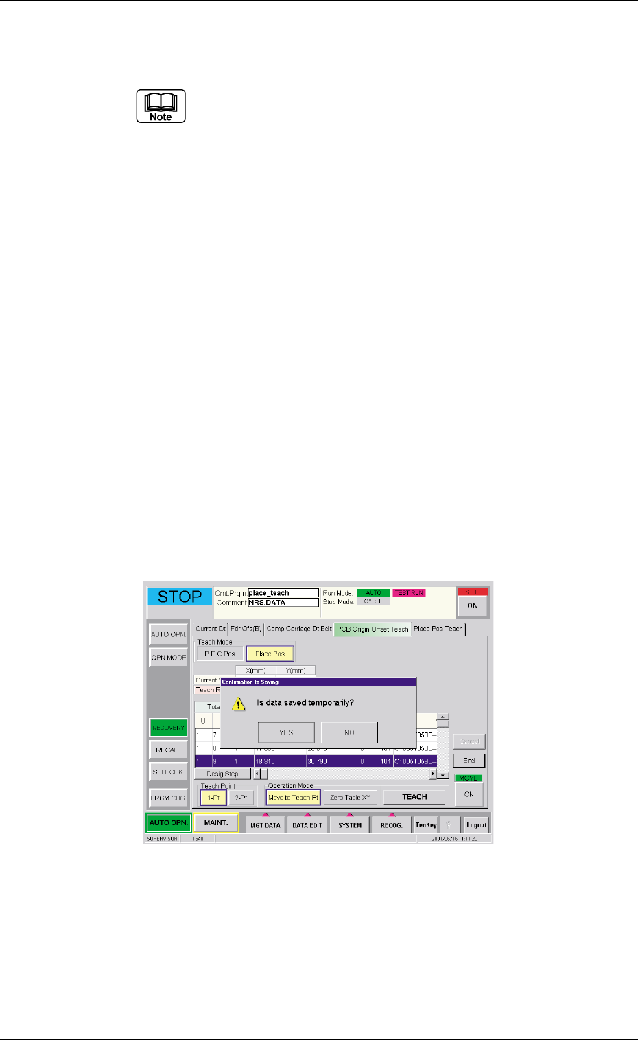
(11) When the new PCB origin offset is entered formally, press the
[End] button *10.
The "Is data saved temporarily ?" window is displayed.
Changing the Current Pattern Program Data (Save)
When the [YES] button is pressed in the "Is data saved
temporarily ?" window, the "Overwrite data. Is it OK ?"
window is displayed.
Press the [YES] button, then the temporarily entered data
about the PCB origin offset will be overwritten.
Fig. 3 "Confirmation to Saving" Window
0301-002
4. PCB Origin Offset Teach