Detailed Circuit Diagram Folder SIPLACE F5.pdf - 第106页
4 Printed Circui t Boards 106 I 0032103 6-010 101FD4 A xis rear panel I (axis 16 6) 0032103 7-010 101FD4 A xis rear panel I I (axis 1 66) 14 7 X6 X5 Star axis 7 20 19 18 17 16 14 13 12 11 10 8 6 5 4 3 9 2 1 7 20 19 18 17…
4 Printed Circuit Boards 105
I
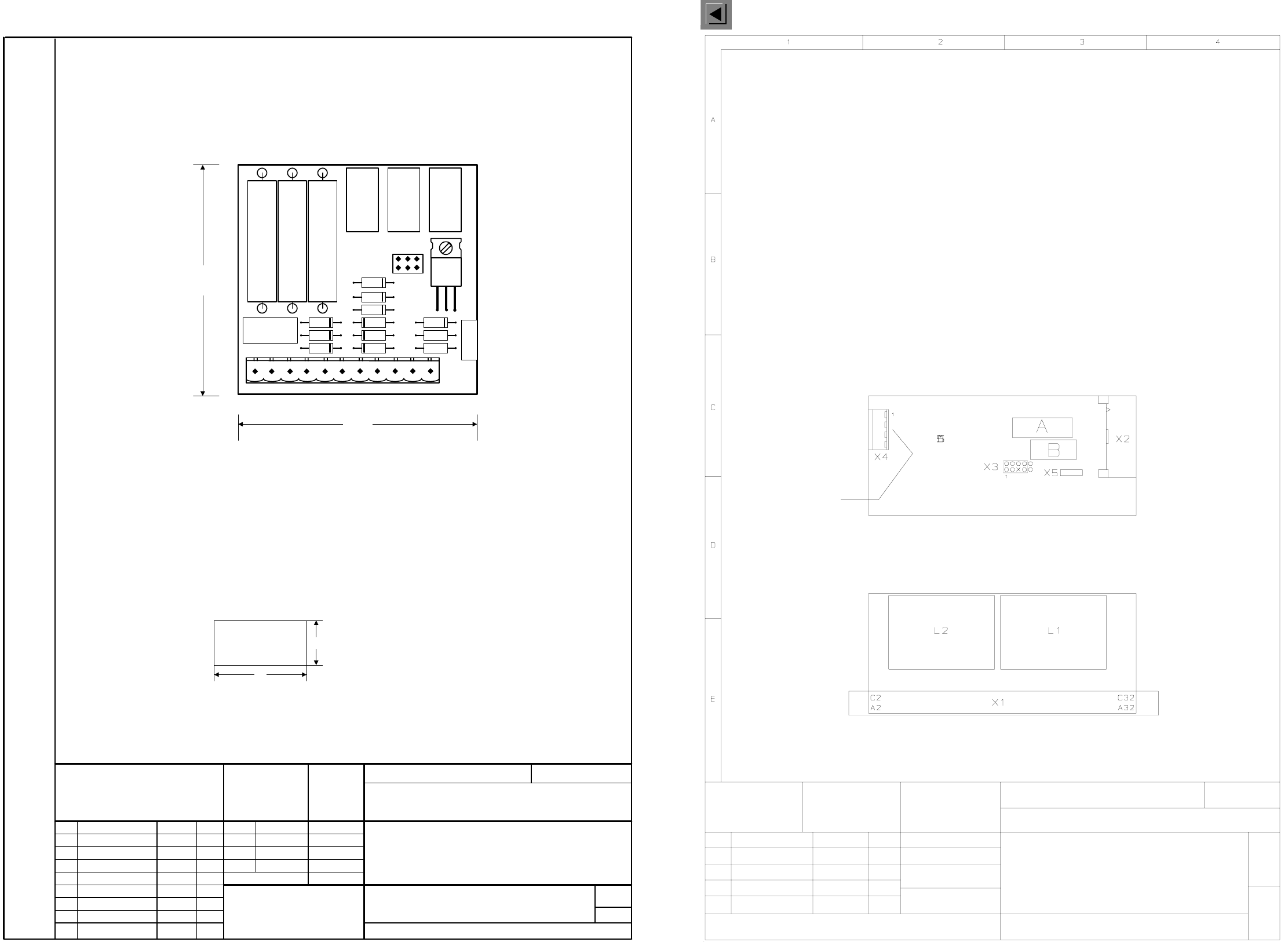
00308443-050101ND4 Discharge board
00320854-020202MD4 745 PC board, backplane - servo Y1002
02 15.04.96
15.04.96 DO
DO
SIEMENS AG
FSZ MUENCHEN
MS-Dorn
03.07.95
00320854-020202MD4
backplane - servo Y1002
745 printed circuit board
SIPLACE
M 1:1
Sheet
1-
Component diagram, bottom
ANL A441 TD FSZ E
DO15.04.96
Component diagram, top
Wire infeed
Apply the following labels:
A: Identification label
Max. component height:
B: Inspection label
Top = 19mm
Bottom = 34 mm
Remove pins marked ’x’
Zust. Modified Date Name
Date
Name
Function status
Product status
Doc. status
02
02
1.
5.
1.
28.05.96
28.05.96
28.05.96 Tu.
Tu.
Tu.
28.05.1996
28.05.1996
00308443-050101ND4
SIEMENS
Aktiengesellschaft
AUT 5 BPB BS1
Datum
Bearb.
Gepr.
Norm
Name
Dateiname:
Zust.
Mitteilung
Datum
Name
(Materialnummer)
Format A4
Mat.-Nr.: FS ES US S/F
Blatt
Maßstab
Weitergabe sowie Vervielfältigung dieser Unterlage, Verwertung und Mitteilung
ihres Inhaltes nicht gestattet, soweit nicht ausdrücklich zugestanden.
Zuwiderhandlungen verpflichten zu Schadenersatz. Alle Rechte für den Fall
der Patenterteilung oder GM-Eintragung vorbehalten.
Copying of this document, and giving it to others and the use or communication
of the contents thereof, are forbidden without express authority. Offenders are
liable to the payment of damages. All rights are reserved in the event of the
grant of a patent or the registration of the utility model or design.
(a1_1zu1.vsd)
00308443.51N
75 mm
72 mm
1/1
R1
K1
R2 R3
K2 K3
V3 V8
V4
V5
V7
V6
V11
V10
V9
V2
R4
R5
A
B
X1
X2
V1
1
Zeichn.Nr.alt:
1710470-Y0034-000-04
Siemens AUT5
00308443-05
AA-BBBB-CCCC
15
10
Function status
Document status
Product status
SMD Placement System Siplace
Discharge board
The following labels have to be stuck on:
A: Identification label
B: Inspection label
Assembly inscription acc. to recommendation VA-F-510-001
font size 1.5 mm, mat. Scotchcal 3698-E ( color A1 Ral 9006 )
AA = manufacturer/location acc. to SN 37040
BBBB = date (year/month/day) acc. to SN 01007
CCCC = numeral
Product inspection certification acc. to recommendation VA Q 509-001
4 Printed Circuit Boards 106
I
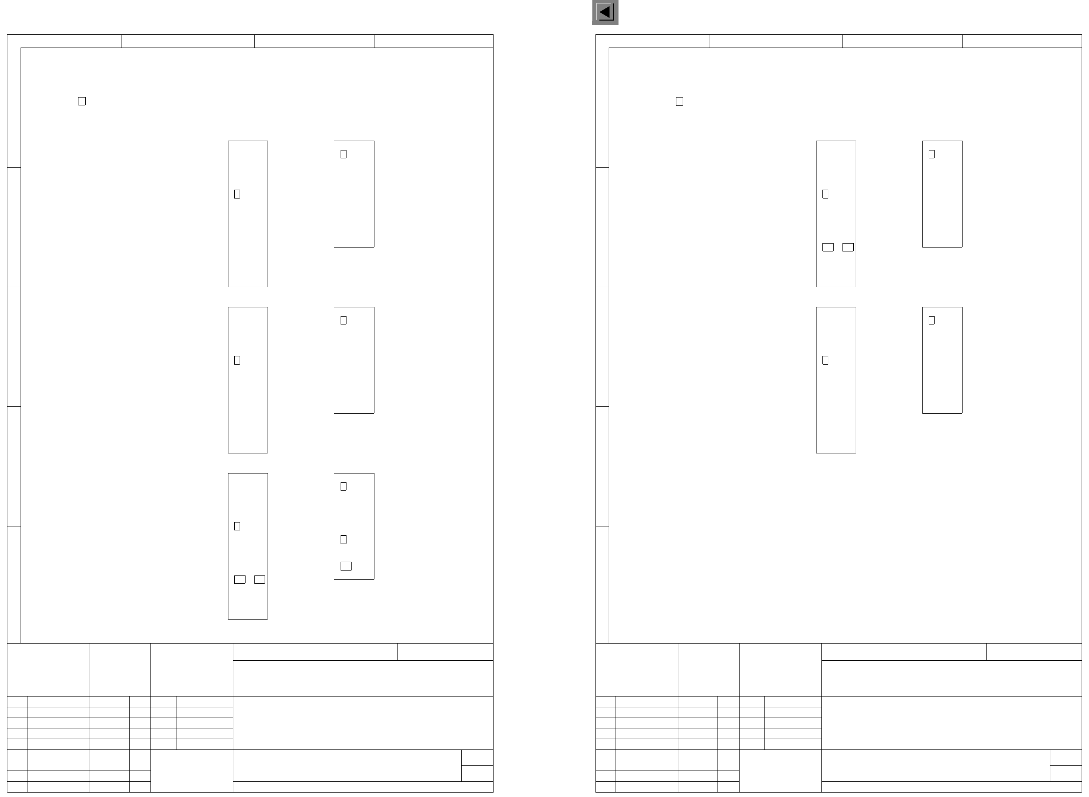
00321036-010101FD4 Axis rear panel I (axis 166)
00321037-010101FD4 Axis rear panel II (axis 166)
14
7
X6X5Star axis
7
2019
1817
16
1413
1211
10
8
65
43
9
21
7
2019
1817
1615
1413
1211
10
8
65
43
9
21
7
2019
1817
1615
1413
1211
10
8
65
43
9
21
15
321036-01
Siemens AG
AUT5-BSM
4321
E
D
C
B
A
XX
XXXX
X
X
X
X
X
X
X
Product status
Doc. status
1
1
SMD Placement System Siplace 80S20
Stat. Modified Date Name
Date
Author
Check.
Stand.
Sh.
Sh.
Scale
Mat. no.:
18.07.1995
Sz
00321036-010101FD4
Axis rear panel I
(axis 166)
1:1
1.
1. Sz
Sz
18.07.95
18.07.95
Remove all key pins marked with
an X from the axis rear panel.
12
9
34
56
8
10
11 12
13 14
7
X2X1X axis
12
9
34
56
8
10
11 12
13 14
7
X4X3Y axis
12
9
34
56
8
10
11 12
13
10
8
65
43
9
21
7
2019
1817
16
1413
1211
10
8
65
43
9
21
15
321037-01
XXXX
X
X
X
X
Siemens AG
AUT5-BSM
4321
E
D
C
B
A
Product status
Doc. status
1
1
SMD Placement System Siplace 80S20
Stat. Modified Date Name
Date
Author
Check.
Stand.
Scale
Sh.
Sh.
Mat. no.:
18.07.1995
Sz
00321037-010101FD4
Axis rear panel II
(axis 166)
1:1
1.
1. Sz
Sz
18.07.95
18.07.95
Remove all key pins marked with
an X from the axis rear panel.
12
9
34
56
8
10
11 12
13 14
7
X2X1Z-SP axis
12
9
34
56
8
10
11 12
13 14
7
X4X3Rotate SP axis
7
2019
1817
1615
1413
1211
4 Printed Circuit Boards 107
I
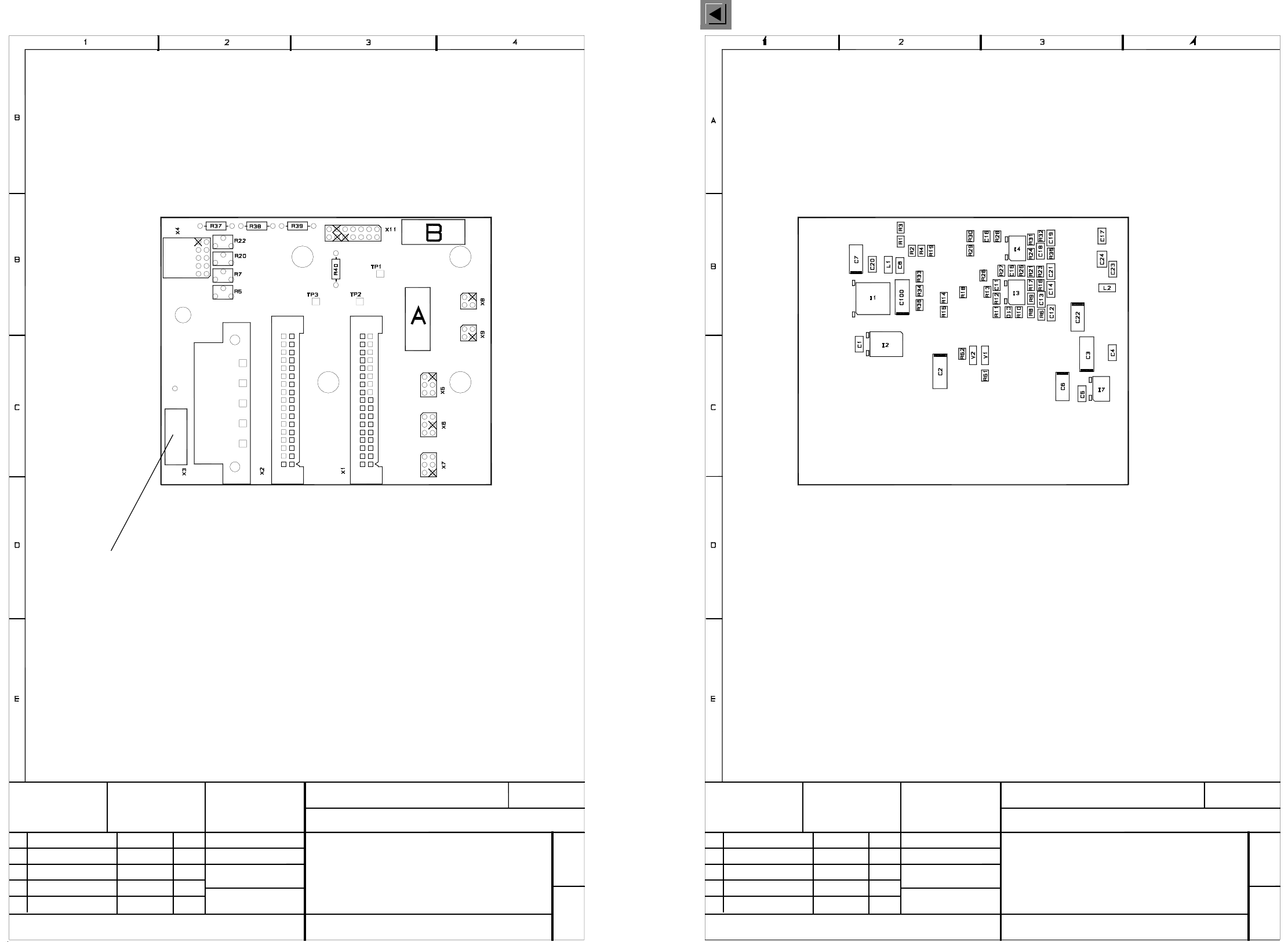
00321189-030101ND4 820 PC board, conversion board, large axis (Sh. 1 of 2)
00321189-030101ND4 820 PC board, conversion board, large axis (Sh. 2 of 2)
Stat.
03
04
Modified
09.10.97
27.03.97
Date
KD
KD
Name
PC board
Dorfner
12.02.97
FSZ MCHN
SIEMENS AG
TD E E
Date
Name
4-layer
G32918 - J2 - B001 - * - 17
Conversion board, large axis
00321189-030101ND4
PC board
Scale
1 : 1
820
1 +
Sheet
Component mounting diagram, component side
Document identification
Remove all pins marked with an X
A = identification label
B = inspection label
03
Stat.
04
Modified Date
27.03.97
09.10.97
Name
KD
KD
TD E E
SIEMENS AG
FSZ MCHN
12.02.97
Dorfner
PC board
Date
Name
00321189-030101ND4
Conversion board, large axis
G32918 - J2 - B001 - * - 17
PC board
Scale
1 : 1
820
Component mounting diagram, solder side
Sheet
2 -