Detailed Circuit Diagram Folder SIPLACE F5.pdf - 第58页
2 Circuit Diagr ams 58 I 0032108 6-050 101LD3 Circuit dia gram, po wer supp ly (Sh . 2 of 2 ) (to K2) +24V DC To S5 input X2kd:1 ye&bn wh&ye Status M odified Stand. Da te Na me O rig. Crea t. f. Cre at. by Author…
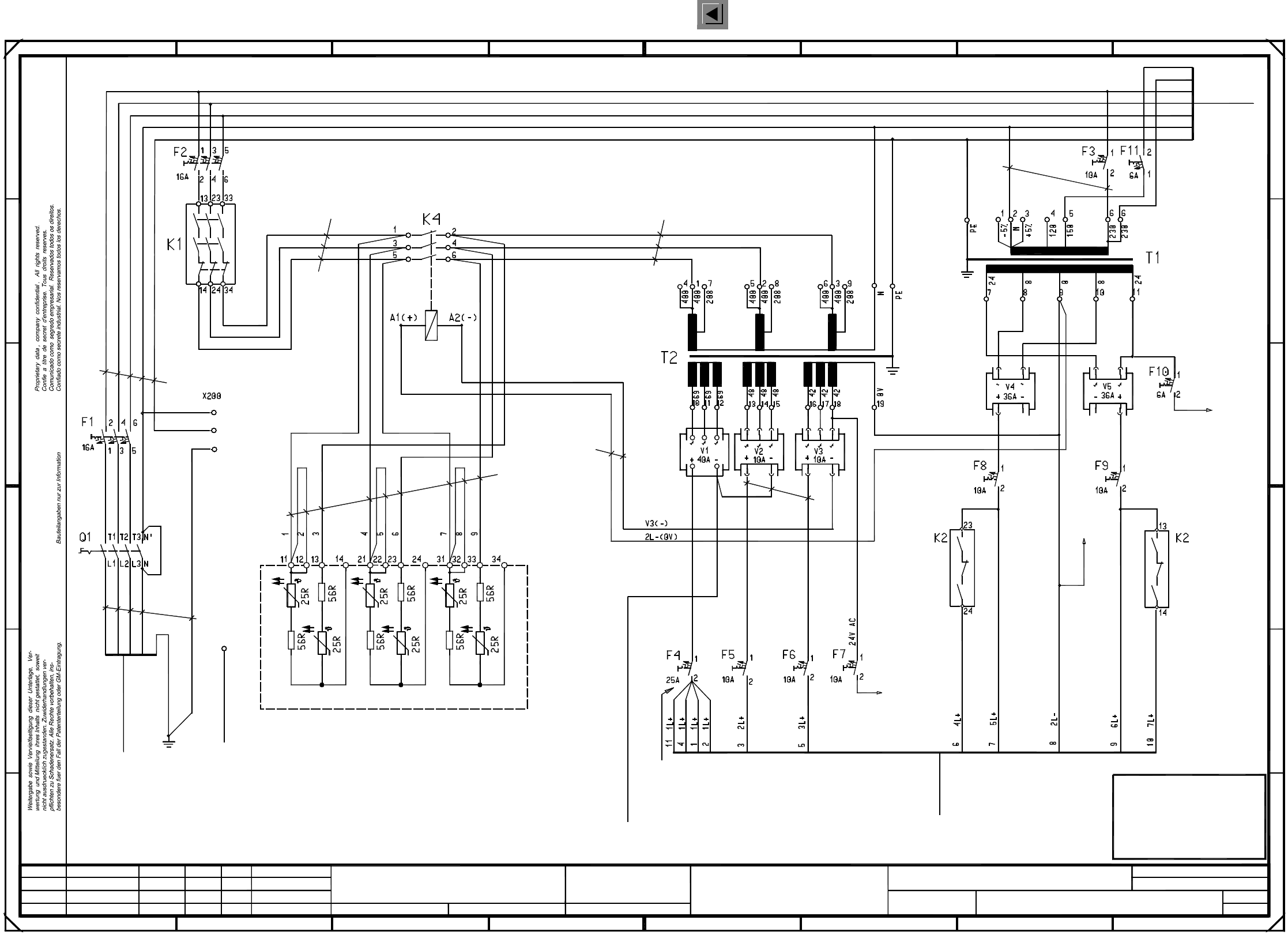
2 Circuit Diagrams 57
I
00321086-050101LD3 Circuit diagram, power supply (Sh. 1 of 2)
6
A
A1
C
D
7
E
F
85
1 45678
A
E
D
C
B
2
B
34
1
1
23
F
2
gnye
bl
bk
bk
bk
bk
bk
2.5mm²
2.5mm²
2.5mm²
bk
1.0mm²
bk
2.5mm² bk
GND
To sheet 2
bk bk
1.0mm²
1.5mm²
To
Terminal panel
*903
00300161-06
rd
gr
br
bk
wh
gnye
bl
Status Modified Date Name Stand.
Author
Check.
Date
Orig. Creat. f. Creat. by
PL EA1 E
Function status
Product status
Document status
SMD Placement System SIPLACE 80S20/F4
Sheet
Sh.
To
Terminal panel
*903
C506-W1
To
*903
Terminal panel
1L- C511-W1
in each sleeve
2 wires
To sheet 2
Emerg.-stop, ext.
C0508-W1 gr
Warning!
24V AC
To sheet 2
bk
If the machine is operated with 230 V
connect the inrush current limiter
(i.e. disconnect wire 3 from 13 and connect it to 14,
in parallel
for the other phases
apply this system as appropriate)
disconnect wire 2 from 12 and connect it to 13,
Inrush current limiter
To
00342917-xx (W1)
Cover
Power supplyPower supply
Base
main power filter 1
To
00342193-xx
2.5mm² gnye
PE
gnye
gnye
2.5mm²
bl
bk
bk
br
2.5mm²
Main
switch
00342917-xx (W3)
Remove jumper, if required (IT net)
(France / Italy / Japan / USA)
Jumper is part of the main switch
PE
PE
N
2.5mm²
bk
bk
bk
1.5mm²
bk
1.5mm²
bk
bk
bk
bk
2.5mm²
bk
br
wh
gnye
bl
(Star/lifting table)
(Tape cutter)
bk
bk
bk
(X/Y-axes)
bk
bk
bk
(X, Y slow)
bk
bk
bk
bk
bk
(Star, slow)
(Lifting table)
(DP1/Z-axes)
bk
bk
bk
bk 4.0mm²
10.0mm²
2.5mm²
bk
bk
bk
bk
bk
bk
bk
bk
bk
bl
gnye
bk
2.5mm²
00321086-050101LD3
Circuit diagram, power supply
#
Tuth
21.07.98
23.01.98
23.01.98
23.01.98
01
01
05
Leh
Leh
Leh
=
SIEMENS AG +
FOR INFORMATION ONLY
This document will
not be replaced when
modifications are made !
2 Circuit Diagrams 58
I
00321086-050101LD3 Circuit diagram, power supply (Sh. 2 of 2)
(to K2)
+24V DC
To S5 input X2kd:1 ye&bn
wh&ye
Status Modified Stand.Date Name Orig. Creat. f. Creat. by
Author
Check.
Date
=
SIEMENS AG
+
FOR INFORMATION ONLY
This document will
not be replaced when
modifications are made !
F F
B
C
D
E
4
D
A
8
1
67
2
2
53 678
12345
E
01
01
05
Leh
Leh
Leh
2
B
A
C
PL EA1 E
00321086-050101LD3
Circuit diagram, power supply
#
Tuth
21.07.98
15.07.98
15.07.98
15.07.98
Function status
Product status
Document status
SMD Placement System SIPLACE 80S20/F4
Sheet
Sh.
GND
To sheet 1
1.0mm²
bk
bk
1.0mm²
To sheet 1
24V AC
F10:2
To sheet 1
24V AC
F7:2
switched
To terminal panel
*904
To sheet 1
1.0mm²
F10:2 24V AC
1.0mm²
To ext. EMERG.-STOP circuit (WPC) gr
gnTo On button
24V AC wh
24V AC br
From EMERG.-STOP circuit (to K1) bl
+24V DC wh&gn
From On button ye
To S5 input X2kd:8 bn/gnControl On
Signaling circuit
Software release
Signaling circuit
To S5 input X2kb:7 wh&gr
Software release To S5 output X2kc:8 gr/bn
Software release To GND, S5 assembly X2kc:M pk&bn
To On button gr&pk
To keyswitch vi
From On button rd&bl
From EMERG.-STOP circuit bk
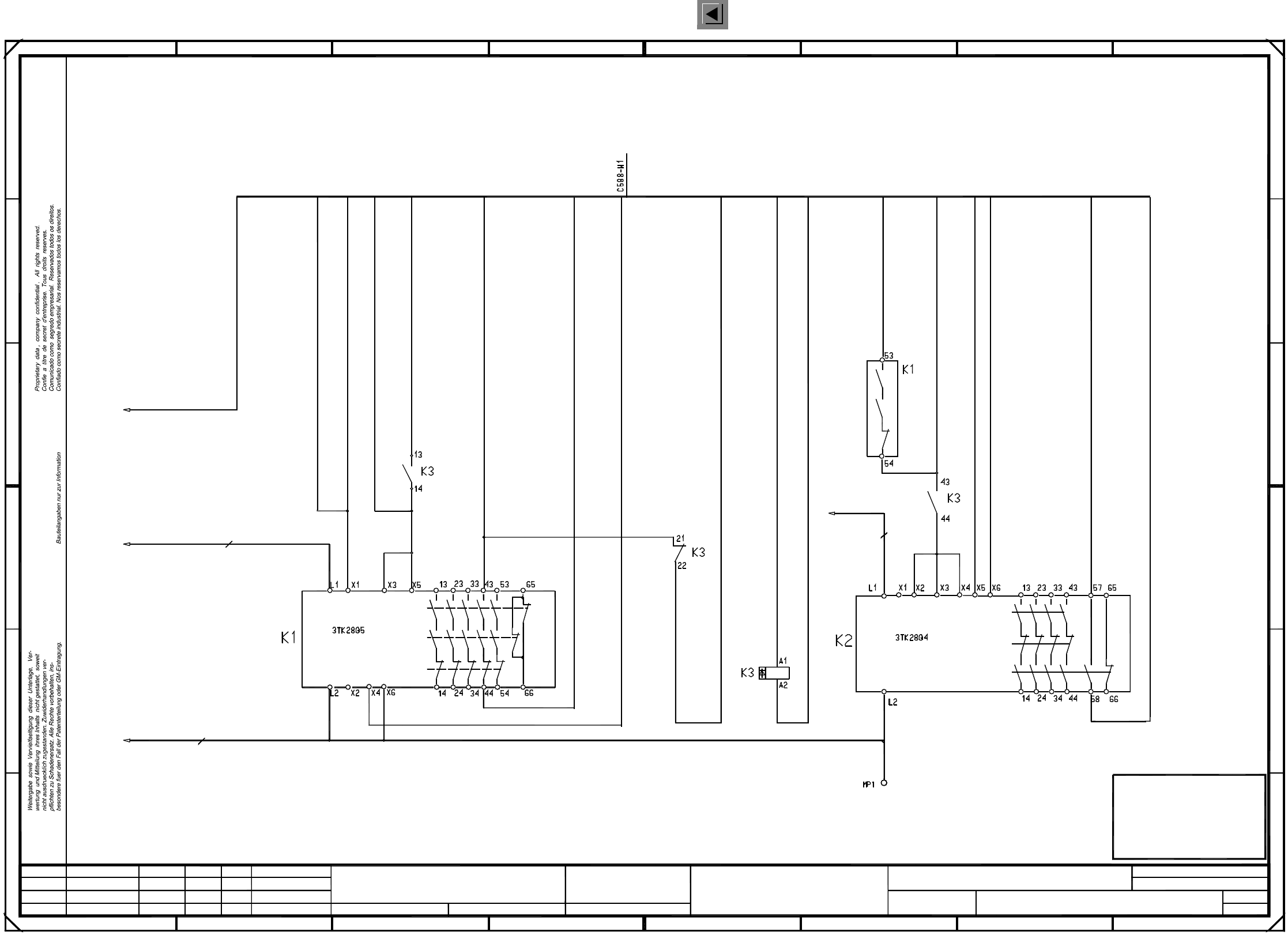
2 Circuit Diagrams 59
I
00321086-050101TD3 Power supply structure (Sh. 1 of 4)
=
SIEMENS AG
+
FOR INFORMATION ONLY
This document will
not be replaced when
modifications are made !
12
12345678
C
D
345
C
B
A
D
1
4
678
A
B
Leh
Leh
05
01
01
23.01.98
23.01.98
23.01.98
21.07.98
Tuth
#
Power supply structure
00321086-050101TD3
E
FF
E
PL EA1 E
Leh
Function status
Product status
Document status
SMD Placement System SIPLACE 80S20/F4
Sheet
Sh.
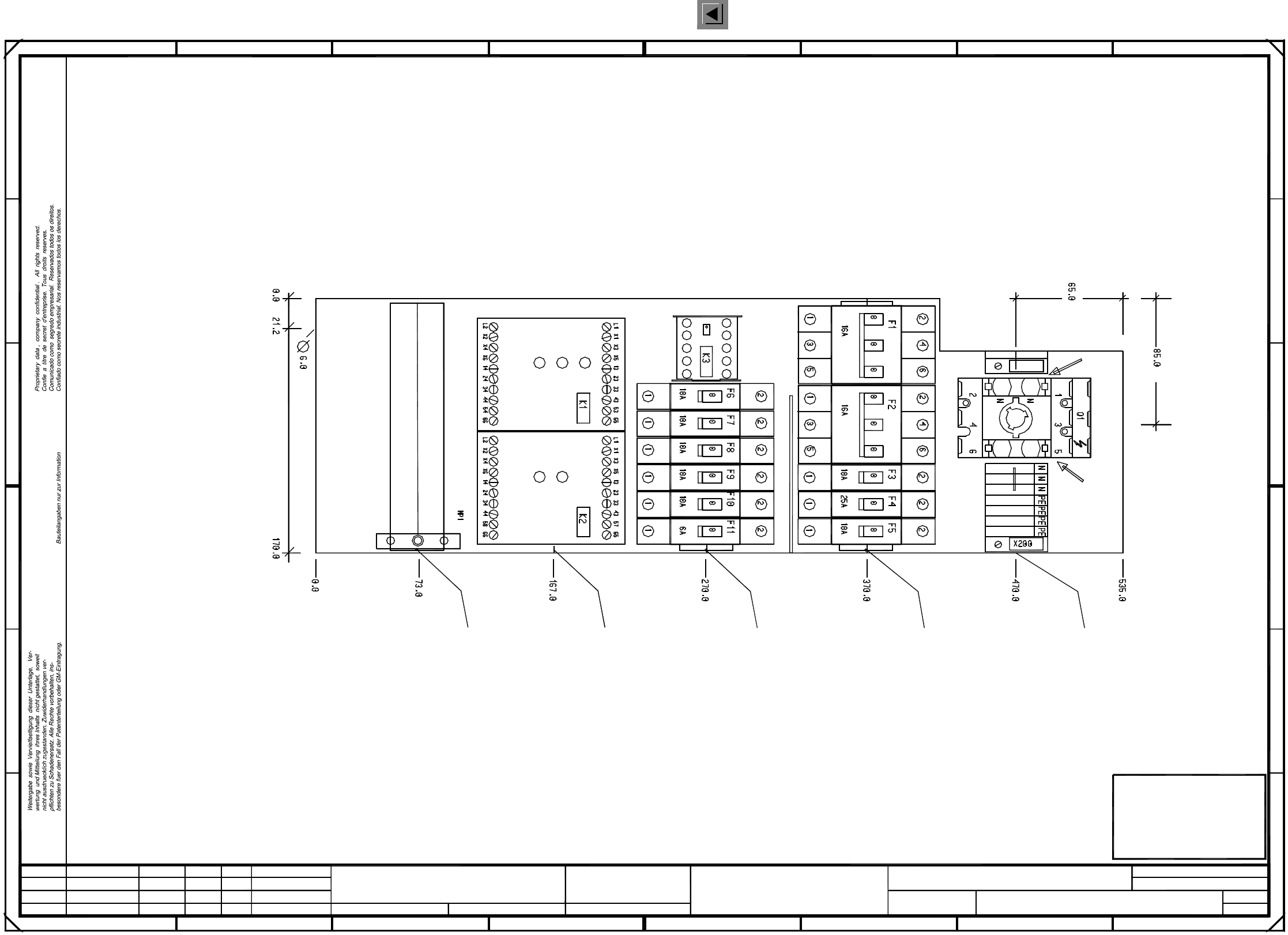
Please note!
Make sure that the X200 terminals on the upper top hat rail are seated with their right end flush with the stop
(This lateral play ensures optimum freedom of movement when pushing the switch
Make sure that the main switch can be moved on the top hat rail for max. 2mm to the left or to the right.
through the front cover.)
TS35 top hat rail
l=160mm
TS35 top hat rail
l=146mm
Ein
On
Ready
Frei
Kanal 1
Channel 1
Channel 2
Kanal 2
Netz
Power
TS35 top hat rail
l=146mm
TS35 top hat rail
l=164mm
TS35 top hat rail
l=130mm
Stand.Status DateModified Name Orig. Creat. f. Creat. by
Author
Check.
Date