Detailed Circuit Diagram Folder SIPLACE F5.pdf - 第37页
1 Detailed Circuit Diagr ams 37 I LP08 PCB c onve yor 2, wi dth adj ustm ent LP8. DW G Str omlau fpla n/C irc uit diagram PL EA Hi 18.12. 2000 SIEMENS Sh. Sh. SMD Placemen t System SIPLACE F5 1 1 PCB conveyor 2 Width adj…
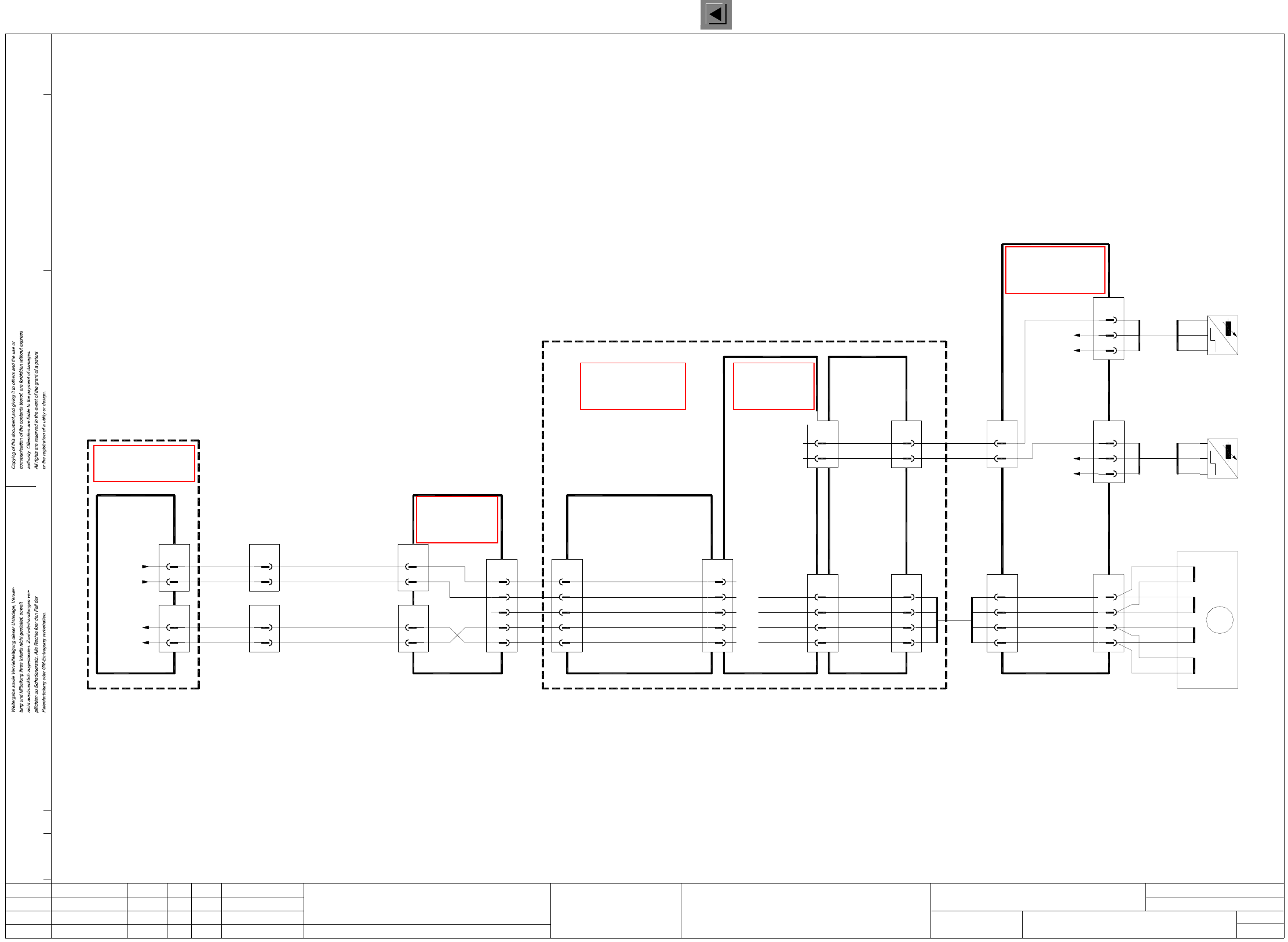
1 Detailed Circuit Diagrams 36
I
LP07 PCB conveyor 2, lifting table control
Stroke 2 B-
Stroke 2 A+
10a,10c
8a,8c
6a,6c
4a,4c
X2b
X1b
18a
17a
4
3
2
1
X4b
12
X3b
10
00325580-xx
Dual stepping
Backplane
wh
br
gn
ye
motor board
Stroke 2 B+
Stroke 2 B-
Stroke 2 A+
Stroke 2 A-
Sensor switch
Lifting table bottom
Sensor switch
Lifting table top
14c
22a
X1b
13c
14a
Dual stepping
00325579-xx
motor board
22c
X3b
20
19
4
5
3
Dual stepping
00325580-xx
Backplane
motor board
Lifting table 2 down
Lifting table 2 fast/slow
End signal, lifting table 2 bottom
End signal, lifting table 2 top
Lifting table 2 up
00326065-xx
(Cable)
X10
20
19
4
5
3
Conversion board
00325581-xx
br
GND
10
X10
+24VDC
X29
2
3
6
bk
br
bl
lifting table 2 bottom
Sensor switch,
00326039-xx
bk
br
bl
A1
+
-
’dual conveyor’
Conversion board
00325581-xx
+24VDC
GND
6
3
bl
br
X27
2
bk
lifting table 2 top
Sensor switch,
bl
br
-
+
00326038-xx
bk A1
X15
2
3
1
orwh
rd
or
4
br
brwh
rdwh
yewh
ye
lifting table 2
00326058-01
Motor
+
-
-
+
+
-
-
+
A
A
B
B
M
12
X11
6
5
7
8
wh
ye
gn
Stroke 2 B+
Stroke 2 A-
LP7.DWG
Stromlaufplan/Circuit diagram
PL EA
Hi
18.12.2000
SIEMENS
Sh.
Sh.
SMD Placement System SIPLACE F5
1
1
PCB conveyor 2
Lifting table control
’Dual conveyor’
X4
5
6
X5
5
6
X4’
X5’
6
5
5
6
conveyor 2
Lifting table 2 down
Lifting table 2 up
conveyor 2
Lifting table 2 top
Lifting table 2 bottom
End signal
End signal
00321778-xx
(Cable)
(Cable)
00321780-xx
Port E5.1
Port E5.0
X4sg
6
X2sg
6
5
5
I/O cards
Port A5.1
Port A5.0
00329285-xx
(Cable)
00329284-xx
(Cable)
00326062-xx
(Cable) (Cable)
00326065-xx
Control unit
00341851-xx
dual conveyor
Control unit -
00327615-xx
Status Modified Date Name Stand.
Check.
Author
Date
Mat. no.:
CAD file:
Orig./Creat. f./Creat.by
See page 65
See page 121
See page 92
See page 121
See page 121
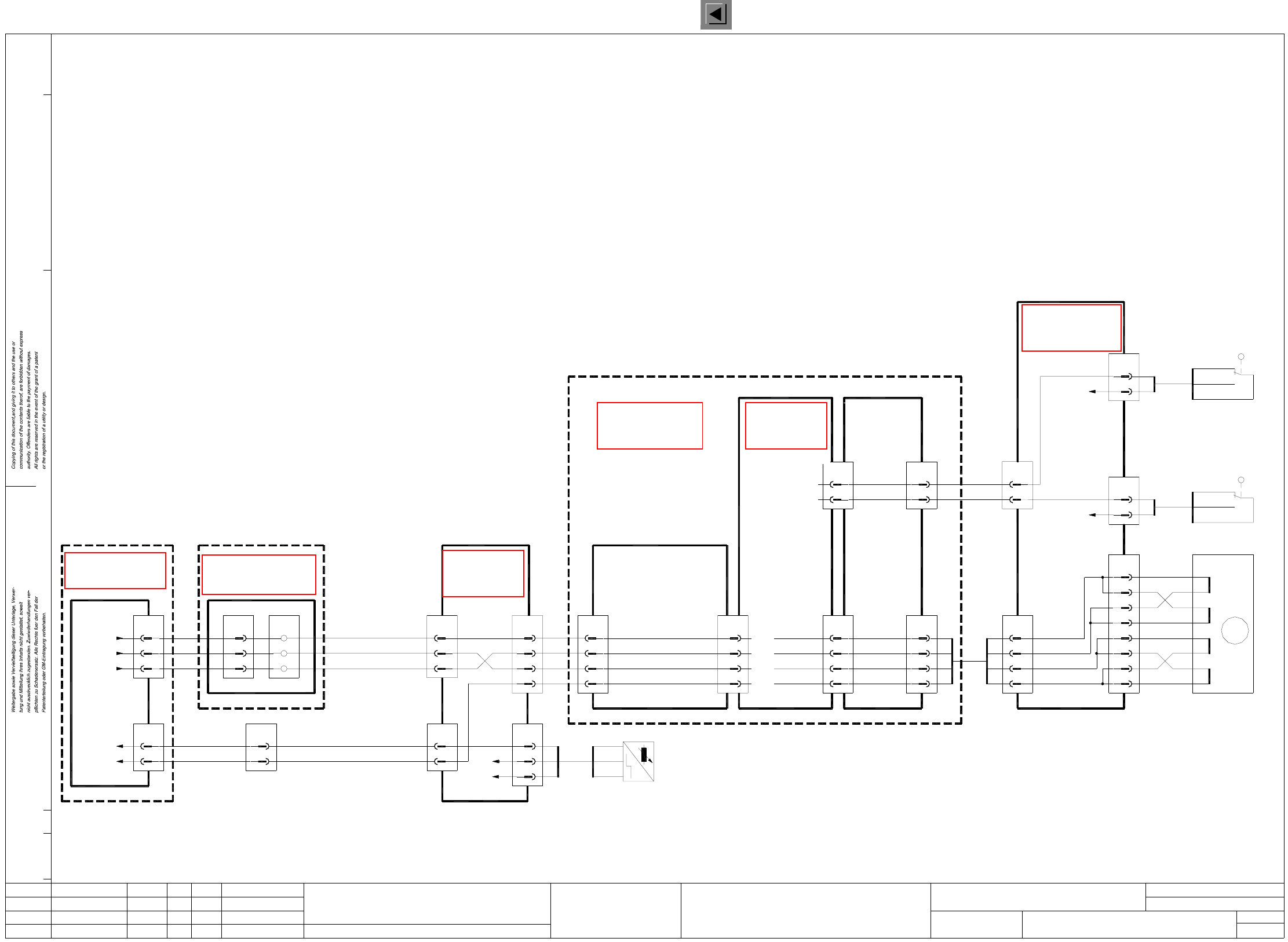
1 Detailed Circuit Diagrams 37
I
LP08 PCB conveyor 2, width adjustment
LP8.DWG
Stromlaufplan/Circuit diagram
PL EA
Hi
18.12.2000
SIEMENS
Sh.
Sh.
SMD Placement System SIPLACE F5
1
1
PCB conveyor 2
Width adjustment
A1bk
bl -
br +
Sensor switch,
wider
End position:
+24VDC
gn
wh
3
4
2
1
adjustment 2
width adjustment 2
Limit switch
width adjustment 2
Limit switch
2
1
4
4
2
1
Control unit -
dual conveyor
00327615-xx
Status Modified Date Name Stand.
Check.
Author
Date
Mat. no.:
CAD file:
Orig./Creat. f./Creat.by
20a/c
18a/c
15a/c
14a/c
X2b
X1b
18c
17c
8
7
6
5
X4b
13
X3b
11
00325580-xx
Dual stepping
Backplane
gr
pk
bl
rd
motor board
Width 1 B-
Width 1 B+
Width 1 A-
Width 1 A+
width adjustment 1
narrower
End position:
width adjustment 1
16a
16c
X1b
15a
Dual stepping
00325579-xx
motor board
21a
X3b
17
9
6
8
Dual stepping
00325580-xx
Backplane
motor board
Width adjstm. 2 fast
Width adjstm. 2 wider
Width adjstm. 2 narrower
End pos., width adjstm. 2
00326065-xx
(Cable)
X25
3
2
Conversion board
00325581-xx
’Dual conveyor’
X4
8
9
X13
9
10
X4’
X1ki X5ki
9
8
10
11
6
7
vi
bk
00344266-xx
left-hand side
Terminal panel
width adjstm., conveyor 2
conveyor 2
Sensor switch: position
End signal: width adjstm.
00320777-xx
(Cable)
(Cable)
00321780-xx
Port E5.4
Port E5.3
X4sg
9
X3sg
11
10
8
I/O cards
Port A6.6
Port A6.5
00321506-xx
(Cable)
00329284-xx
(Cable)
00326062-xx
(Cable) (Cable)
00326065-xx
Control unit
00341851-xx
A6
5
rd
9
9
Port A6.4
8
6
9
8
X10
6
17
+24VDC
GND
fast, conveyor 2
Motor, width adjustment
Motor, width adjustment
narrower, conveyor 2
Motor, width adjustment
wider, conveyor 2
Position width adjustment 2
00326035-xx
bk
br
bl
rd
11
X10
+24VDC
X33
2
3
narrower
00326037-xx
br
gn
wh
’dual conveyor’
Conversion board
00325581-xx
3
2
wh
gn
X31
wider
wh
gn
00326036-xx
br
X17
6
7
5
orwh
rd
or
8
br
brwh
rdwh
yewh
ye
width
00326056-xx
Motor
+
-
-
+
+
-
-
+
A
A
B
B
M
13
X11
2
1
3
4
bl
pk
gr
Width 1 B+
Width 1 A-
Width 1 B-
Width 1 A+
See page 92
See page 121
See page 121
See page 86
See page 65
See page 121
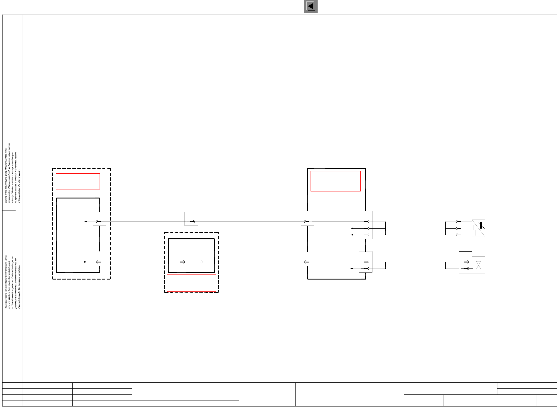
1 Detailed Circuit Diagrams 38
I
LP09 PCB conveyor 2, ceramic substrate centering
(Cable)
00329284-xx
Conversion board
00325581-xx
’dual conveyor’
6
2
br
X49
GND
+24VDC
6
3
bl
br
2
X47
bk
12
Terminal panel
left-hand side
00344266-xx
X4’
X1ki
12
12
8
A6
X5kiX3sg
12
X4sg
00321506-xx
(Cable)
Port A6.7
Port E5.7
00341851-xx
Control unit
X13
12
X14
LP9.DWG
Stromlaufplan/Circuit diagram
PL EA
Hi
18.12.2000
SIEMENS
Sh.
Sh.
SMD Placement System SIPLACE F5
1
1
PCB conveyor 2
Ceramic substrate centering
12
00321780-xx
(Cable)
00320777-xx
(Cable)
bl
rd-bl
Sensor switch
Valve, ceramic substrate centering 2
Ceramic substrate centering 2
Ceramic substrate
Sensor switch
bk
GND
br
bl -
+
bk A1
(Cable)
00326051-xx
B1
2
1
X40
br
wh
00326049-xx
Valve
centering 2
centering 2
Ceramic substrate
Status Modified Date Name Stand.
Check.
Author
Date
Mat. no.:
CAD file:
Orig./Creat. f./Creat.by
See page 65
See page 86
See page 121