Detailed Circuit Diagram Folder SIPLACE F5.pdf - 第84页
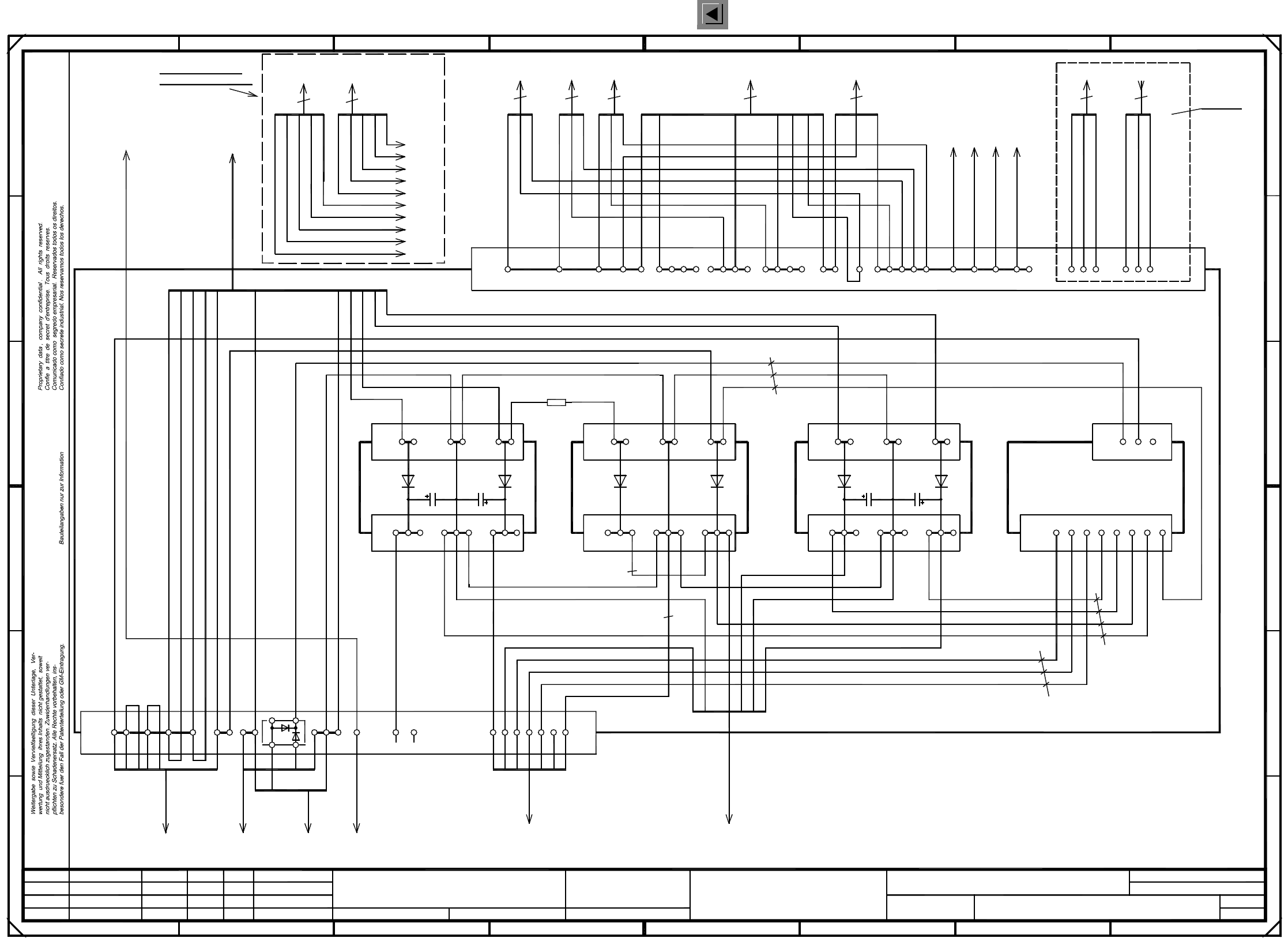
2 Circuit Diagr ams 84 I 0032151 0-070 201 TD3 T ermin al panel, r ight-ha nd si de = SIEMEN S AG + L3 N 1 X 18 X X XX X C 23 4 7 L1 56 X207 A 10 10 N N X 13 17 18 6 11 12 19 X X X PE B A 420,0 mm F L2 X2rd L3 L3 X1re 4 …
2 Circuit Diagrams 83
I
00321510-070201LD3 Circuit diagram, terminal panel, right-hand side
456 78
17
2L+
9
X206:L1
3456
X206:L2
(rd) (re)
X2
X1
1
(K1)
34 56
123 456 7
1mm²
N
X2
X2
PEPEPEPE
X1
12
NN
56
L2 L3L1
3
L1 4L3 L3L2L2 6
1413 15 16
2L+
1L+ 11
12
1L+ 2
2L+ 3
10mm²
1mm²
89
(rc)
6
4
X206
X207
1
5
C0530
2
Y636-
Y636-
C0530
C938
5L+
PE PE
1L+
1L+
1L+
1L+
(rb)
PEPENN 5
(+24V)
L1
2L+/5L+
2L+/5L+
2L-
1L-
1L+ 4
1L+ 1
7
10mm²
C510-W1
6
3
3
2
6mm²
6mm²
C709
C708
X31
*938/X16
2L+
2L-
2
9
8
D
7
C
A
6
D620-W1
10
8
3
5
56
1mm²
F
342
2
B
A
1
1
1
8
4L+
18 8 8
1mm²
5
10 19 11
1
4
72345
12
X1
12398711
4
76
3
C
D
E
00344540
E
F
00344539
4
1mm²
7
X1
PEN5PEN4
-xx-xx
C511-W1
10 10
6
6L+ 9
7L+ 10
2L+/5L+
3
1
2L-
5
2
1mm²
2L-
C560
6
1
7
3
21
6
L3 PE
*904/X211,X212
K504-W1
(K2)
*935/X3
Y510-W1
*935/X2
C509-W1
2L- 8
D619-W1
(K1)3L+ 5
X206:PE
X206:N
X206:L3
X206:L2
X206:L1
X206:PE
X206:N
X206:L3
18
89
A2
A3 A4 A5
34
L1 L2
R1
21
PL EA1 E
Function status
Product status
Document status
SMD Placement System SIPLACE 80S20/F4
Sheet
Sh.
Status Modified Date Name Stand.
Check.
Author
Date
Orig. Creat. f. Creat. by
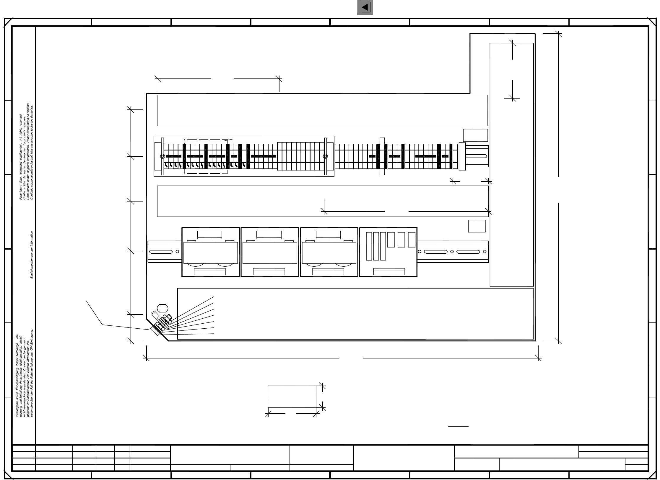
Terminal panel, righthand side
Terminal panel
To
Servo unit
To
Servo unit
To
Tape cutter 1
To To
Tape cutter 2
To
Servo
Star point 007
wh
bl&bk
bl&bk
bl&bk
0.5mm²
6L+ unswitched
+7L switched
+7L switched
6L+ unswitched
4.7 Ohm / 5W
bk
bk
1.0mm²
1.5mm²
To
To
WPC interface
righth. side D911
lefth. side, D910
WPC interface
Power supply
To
Power supply
VI rectifier
To
in SIPLACE 80F4 machines only
WPC interface:
ToToTo
Control unit Interface Interface
lefth. side, C955 righth. side C956
To
Power supply
Power supply
SC
To
Option:
From UPSTo UPS
br
br
gn
gn
wh
wh
bk bk
wh
gr
bk
1.5mm²bk
br
gn
ye
gr
pk
bl
wh
Spare
bl&bk
bl&bk
bl&bk
gn
bk bk
wh
wh
gn
gn
wh
wh
wh
gn
ye
gr
wh
br
br
gr
ye
wh
pk
gr
bk
gn&ye
gn&ye
bk
gn&ye
gn&ye To servo unit
To control unit
To cable
To cable
br
bl
gn&ye
br
bl
gn&ye
wh
pk
bk
wh
wh
bl
br
gn&ye
bl
bkbk
bl
bl
bl
rd
br
gr
wh
br
br
br
gn&ye
gn&ye
gn&ye
gn&ye
gn&ye
bl
br
gr
gn&ye
rd
wh
br
wh
wh
gn&ye
br
bl
gn&ye
gn&ye
bl
bk
br
bk
gn&ye
bk
bk
br
bk
bl
When using
a UPS, connect
the cables and
remove jumper
X206:4-5 !
=
SIEMENS AG
+
00321510-070201LD3#
Tuth
21.10.98
08.06.98
01.06.00
21.10.98
01
02
07
Leh
Tu.
Leh
C523-W100300161-06Y511-W1 C516 C517
C506-W1
*952
1
X1
11
4
1
2
(K1)
2
12V
4
6
2L-
1mm²
1mm²
1mm²
C935
5
7L+ 10
6L+ 9
PE
2
(K2)
5
2
1L-
B
2
(K2)
(+24V)
4
1
1
456
123
2 Circuit Diagrams 84
I
00321510-070201TD3 Terminal panel, right-hand side
=
SIEMENS AG +
L3
N
1
X
18
XX
XX
X
C
234 7
L1
56
X207
A
10
10
N
N
X
13
17
18
6
11
12
19
X
X
X
PE
B
A
420,0mm
F
L2
X2rd
L3
L3
X1re
4
D
E
F
C
X
14
15
16
5
315,0mm
5
D
L2
2
B
C
5
6
4
PE
PE
10
X1rc X1rd
XX
2 6
PE
PE
PE
A4
A5
X2rb X2rc
3
X1rb
AA-BBBB-CCCC
N
PE
PE
00321510-07
SIEMENS PLEA 1
A
B
1
END
E
D
500,0mm
XX
XXX
L1
78
252,0mm
190,0mm
N
L2
8
XX
X206
1
8
9
3
L1
L1
PE
PE
N
40
20
4
A2 A3
1
7
8
1
L3
01
01
07
Leh
Leh
Leh
XX
116,0mm
XX
L2
PL EA1 E
00321510-070101TD3
#
Tuth
21.10.98
08.06.98
08.06.98
21.10.98
Function status
Product status
Document status
SMD Placement System SIPLACE 80S20/F4
Sheet
Sh.
Length for cable ducts +/- 5mm !
Please note:
Terminal panel, righthand side
Font size: 2.5mm, material: Scotchcal 3698-E (color: A1 RAL 9006)
BBBB = date (year/month/day) acc. to SN 01007
AA = manufacturer/location acc. to SN 37040
Assembly inscription acc. to VA - F - 510 - 001 guideline
CCCC = series number
Creat. by
D: space for voltage label from NAFTA – label set (for USA only)
B: inspection label
A: identification label
C: ground label
Identification: testing engineer, month, year
Orig. Creat. f.Stand.
Check.
Author
Date
NameDateModifiedStatus
The following labels have to be applied:
to 4L+ (8V),
This way you will switch from 1L+ (100V)
and insert it at X207 11-12-13-14-15.
remove the jumper from X207 13-14-15-16-17
- when commissioning the X,Y axes the first time
thus reducing the crash risk.
Please note:
Ground connection
acc. to constructions specs 00343603, sh.2
0.0mm
35.0mm
Screw
SN 70093 contact washer
DIN 439 nut
Annular cable lug
DIN 125 washer
DIN 7980 split washer
DIN 439 nut
Please note: Break off one rib at each X !
Cable duct: 65x66 l=460mm
Cable duct: 65x66 l=340mm
Please note: break off one rib at each X !
80.0mm
30.0mm
230.0mm
Cable duct: 65x46 l=400mm
Please note: Break off one rib at each X !
Cable duct: 65x46 l=400mm
Please note: Break off one rib at each X !
110.0mm
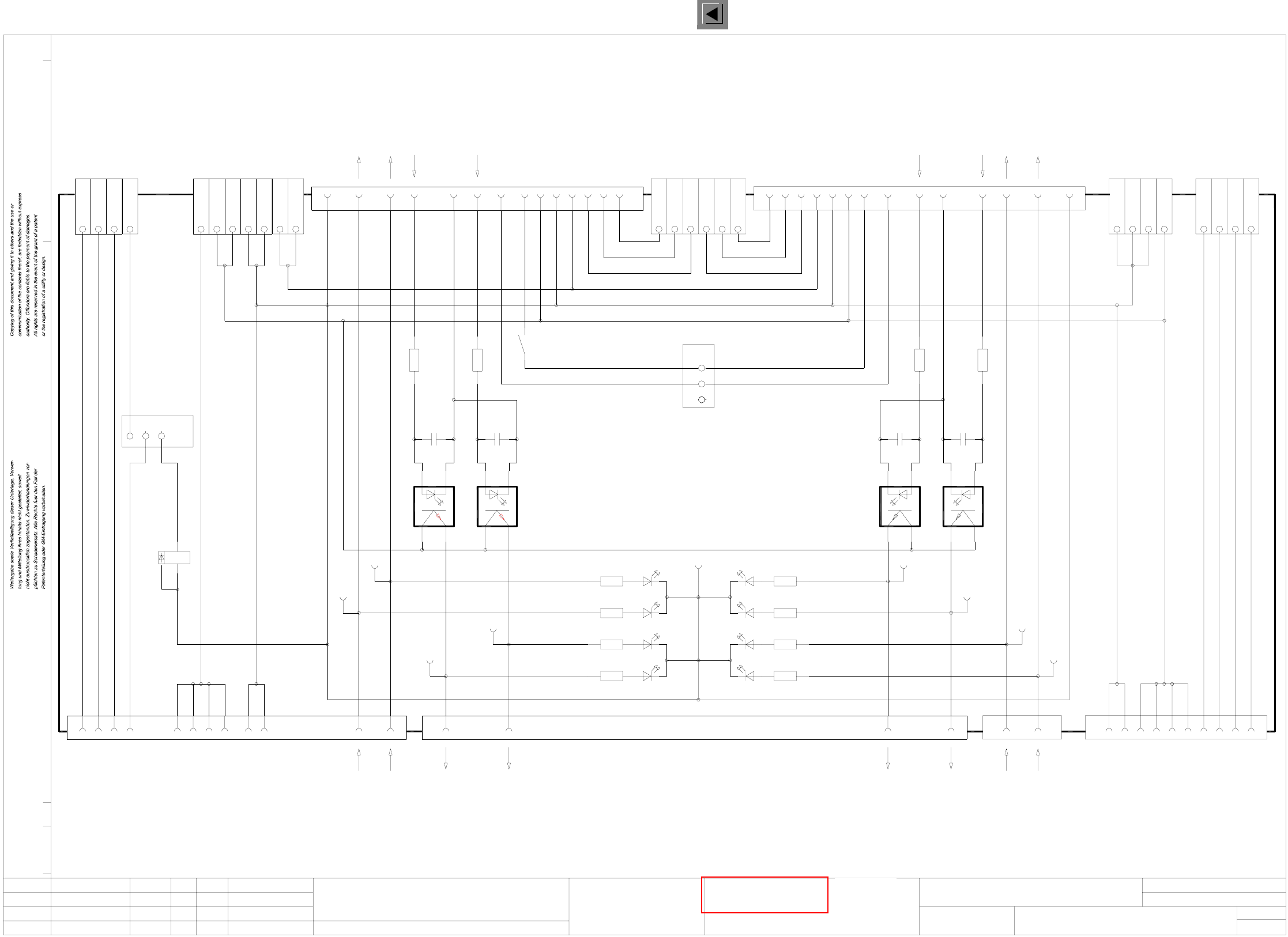
2 Circuit Diagrams 85
I
00200034-030101LD3 Optical decoupling unit
34
12
+-
+-
+-
+-
34
21
34
21
Name Norm
Beab.
Urspr./Ers.f./Ers.d.
Bl.
Bl.Stromlaufplan/Circuit diagramDatumAenderungZustand
Datum
Gepr.
1816151413121110987654321 17
CAD-Datei :
Mat.-Nr. :
SIEMENS
AUT 5
Product status
Doc. status
SMD Placement System Siplace 80S
1
1
29.10.1990
Tekin
Optical decoupling
unit
1. Tu.
14.06.96
GND 24V
X1 9
K1
13
6
9
1 2 3
JP2
X5 8
1413
GND 24V
GND 24V
10 11 12
5
6
7
X5
X5
X5
GND 24V
Received
Permission
151413X3
65
Permission
Received
MP2
MP1
1K5 1,1W
R1
0,1uF
C1
Request
GND n-1
19 20
Request
U1
MP4
GND 24V
11
loop
K1
1
7
Fault signal
12
1K5 1,1W
R2
0,1uF
C2
Transferred
18
previous station
To
U2
6
Transferred
2K7
R8
2K7
R7
MP3
2K7
R5
2K7
R6
Permission
Received
Transferred
Request
+24VDC
Spare
Spare
Spare
1098
+30VDC unswitched
+24VDC
123
GND 24V
X7
X7
X7
X7
X7
1
2
3
4
5
6X7
Spare
Spare
Spare
Spare
Spare
Spare
1
2
3
JP1
MP9
V2
+-
V1
+-
V3
+-
V4
+-
ye
ye
gn
gn
gn
gn
ye
ye
V8
V7
V5
V6
Spare
Spare
Spare
9810X4
+24VDC
GND 24V
+30VDC unswitched
564
2K7
R11
2K7
R12
2K7
R10
2K7
R9
Permission
Transferred
Request
Received
11
Fault signal
12
loop
following station
To
1K5 1,1W
R3
0,1uF
C3
Permission
15
7
Permission
U3
MP5
GND 24V
1K5 1,1W
R4
0,1uF
C4
Received
GND n+1
1413
8
Received
U4
MP6
Request
GND 24V
Transferred
18 19 20
7
Transferred
Request
MP7
MP8
X1 8X2 5
Tu.
14.06.96
3.
Output 1
Output 2
Output 3
Output 4Output 4
Output 3
Output 2
Output 1
6
7
8
X6
X6
X6
5 X6
12111091234
+ X6
+24VDC
+24VDC
+24VDC
+24VDC
Input 1
Input 2
Input 3
Input 4 Input 4
Input 3
Input 2
Input 1
+24VDC
U
U
X5
X5
P
P
M
X5
X5
X5
M X5
+30VDC unswitched
+30VDC unswitched
GND 24V
GND 24V
+24VDC
+24VDC
G X5
1234
GND 24V
GND 24V
GND 24VX6
X6
X6 -
-
-
GND 24V
GND 24V
X2 13 14
+30VDC switched
+30VDC switched
+30VDC switched
+30VDC switched
+30VDC switched
00200034-030101LD3
1.
Tu.
14.06.96
Function status
00200034
00200034-03
34
12
Siehe Seite 102