IPC 7711A.pdf - 第215页
OUTLINE This method is used to repair cosmetic defects or minor damage to an unsupported tooling or mounting hole. The hole may have component leads, wires, fasteners, pins, terminals or other hardware run through it. Th…

3. If the printed wiring board is warped along more than one edge or more than one
plane, clamp the entire printed wiring board to the base plate.
4. Place the printed wiring board, restraint bars and base plate into the oven. Bake
for 1 hour at 125°C.
NOTE
If possible, after the 1 hour bake cycle, shut off the oven and leave the printed
wiring board inside. This will allow the printed wiring board to slowly cool to room
temperature improving stress relief.
5. Remove from the oven and allow to cool to room temperature.
6. Remove restraint bars.
7. Check the edges deflection using a caliper or pin gauges.
EVALUATION
1. Check for marks or damage along edges.
2. Electrical tests as applicable.
NOTES
IPC-7721A
Number: 3.2
Revision:
Date: 2/98
Subject: Bow and Twist Repair
Page2of2
Copyright Association Connecting Electronics Industries
Provided by IHS under license with IPC
Not for Resale
No reproduction or networking permitted without license from IHS
--``,``,-`-`,,`,,`,`,,`---
OUTLINE
This method is used to repair cosmetic defects or minor damage to an unsupported
tooling or mounting hole. The hole may have component leads, wires, fasteners,
pins, terminals or other hardware run through it. This repair method uses high
strength epoxy to restore the damaged surface surrounding the hole. This method
can be used on single sided, double sided or multilayer printed wiring boards and
assemblies.
CAUTION
Damaged inner-layer connections may require surface wire adds.
REFERENCES
2.1 Handling Electronic Assemblies
2.2 Cleaning
2.5 Baking and Preheating
2.6 Epoxy Mixing and Handling
TOOLS & MATERIALS
Ball Mills
Cleaner
Color Agent, Various Colors
Epoxy
Hand Held Drill
Polyimide Tape
Knife
Mixing Sticks
Oven
Wipes
PROCEDURE
1. Clean the area.
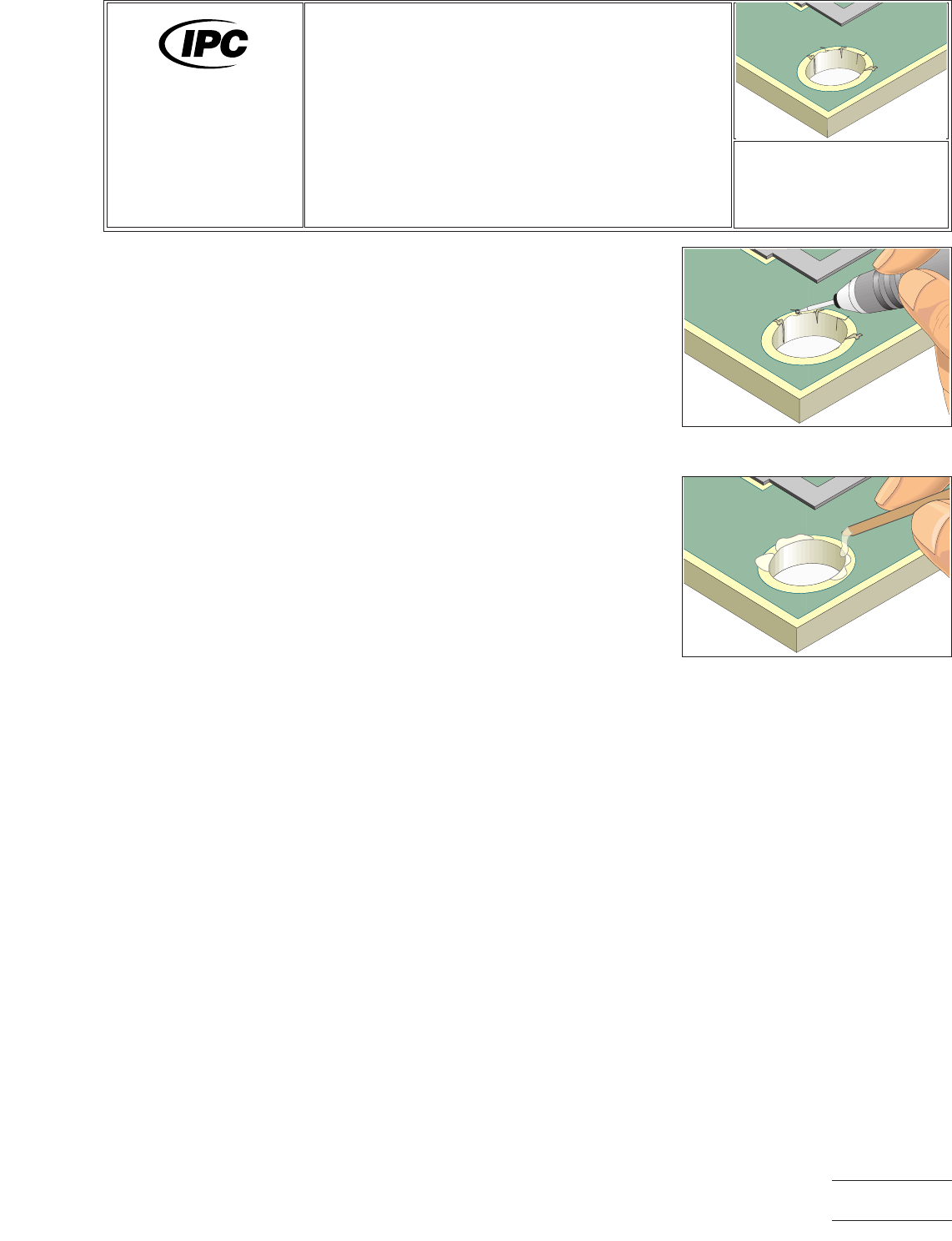
2. Mill away the damaged board base material using the hand held drill and ball
mill. All damaged base board material and solder resist must be removed. No
fibers of laminate material should be exposed at the surface peremiter of the
hole. (See Figure 1.)
NOTE
To clearly see that all damaged material has been removed, flood the area with
alcohol or solvent. Damaged internal fibers of the base material will show up
clearly.
3. Remove all loose material and clean the area.
4. Where needed, apply Polyimide tape to protect exposed parts of the printed
wiring board. Tape may be required inside the hole. If epoxy reduces the inside
diameter, the hole may have to be redrilled after the epoxy has cured.
NOTE
The printed wiring board may be preheated prior to filling the area with epoxy.
A preheated printed wiring board will allow the epoxy to easily flow and level out.
Figure 1 Mill away damaged material.
Figure 2 Apply epoxy with a small
wood stick sharpened at one end.
7721A
Repair and
Modification of
Printed Boards and
Electronic Assemblies
Revision:
Date: 2/98
Hole Repair,
Epoxy Method
Number: 3.3.1
Product Class: R, W
Skill Level: Advanced
Level of Conformance: High
Material in this manual was voluntarily established by Technical Committees of IPC. This material is advisory only and its use
or adaptation is entirely voluntary. IPC disclaims all liability of any kind as to the use, application, or adaptation of this material.
Users are also wholly responsible for protecting themselves against all claims or liabilities for patent infringement. Equipment
referenced is for the convenience of the user and does not imply endorsement by IPC.
Page1of2
Copyright Association Connecting Electronics Industries
Provided by IHS under license with IPC
Not for Resale
No reproduction or networking permitted without license from IHS
--``,``,-`-`,,`,,`,`,,`---

Epoxy applied to an unheated printed wiring board may settle below the printed
wiring board surface as the epoxy cures.
CAUTION
Some components may be sensitive to high temperatures.
5. Mix the epoxy. If desired, add color agent to the mixed epoxy to match the
printed wiring board color.
6. Coat the area with epoxy up to and flush with the printed wiring board surface.
A small wood stick may be used to apply and spread the epoxy. (See Figure 2.)
NOTE
A slight overfill of epoxy may be desired to allow for shrinkage when epoxy
cures.
7. Cure epoxy per the manufacturers recommended instructions.
8. After the epoxy has cured, remove the tape.
9. If needed, use the knife or scraper and scrape off any excess epoxy. Scrape
until the new epoxy surface is level with the surrounding printed wiring board
surface.
NOTE
Apply surface coating to match prior coating as required.
10. Remove all loose material. Clean the area.
EVALUATION
1. Visual examination for texture and color match.
2. Hole size measurement to specification
3. Electrical tests to conductors around the repaired area as applicable.
NOTES
IPC-7721A
Number: 3.3.1
Revision:
Date: 2/98
Subject: Hole Repair, Epoxy Method
Page2of2
Copyright Association Connecting Electronics Industries
Provided by IHS under license with IPC
Not for Resale
No reproduction or networking permitted without license from IHS
--``,``,-`-`,,`,,`,`,,`---