IPC 7711A.pdf - 第303页
OUTLINE This procedure covers the use of an eyelet for the repair of a damaged pad on a hole that has an inner layer connect. CAUTION This procedure is used to restore the integrity of a through connection on a multi- la…

NOTES
IPC-7721A
Number: 5.1
Revision:
Date: 2/98
Subject: Plated Hole Repair, No Inner Layer Connection
Page4of4
Copyright Association Connecting Electronics Industries
Provided by IHS under license with IPC
Not for Resale
No reproduction or networking permitted without license from IHS
--``,``,-`-`,,`,,`,`,,`---
OUTLINE
This procedure covers the use of an eyelet for the repair of a damaged pad on a hole
that has an inner layer connect.
CAUTION
This procedure is used to restore the integrity of a through connection on a multi-
layer PC board, having an inner layer connect, but ONLY if the full barrel of the
plated through hole remains intact. If there is barrel damage see appropriate proce-
dure.
CAUTION
This method will reduce the inside diameter of the hole. The minimum hole size
requirement must be checked for acceptance.
REFERENCES
2.1 Handling Electronic Assemblies
2.2 Cleaning
TOOLS & MATERIALS
Ball Mills, Carbide
Buffer
Caliper
Eyelets
Eyelet Press System
Eyelet Repair Kit
Eyelet Setting Tools
Hand Held Drill
Liquid Flux
Knife
Microscope
Pin Gauges
Solder
Solder Iron
Wipes
EYELET SELECTION CRITERIA
Figure 1 Insert the eyelet into the
hole.
Figure 2 Set the eyelet using an
eyelet press.
Figure 3 Completed repair.
7721A
Repair and
Modification of
Printed Boards and
Electronic Assemblies
Revision:
Date: 2/98
Plated Hole Repair,
Double Wall Method
Number: 5.2
Product Class: R, F, W
Skill Level: Advanced
Level of Conformance: Medium
Material in this manual was voluntarily established by Technical Committees of IPC. This material is advisory only and its use
or adaptation is entirely voluntary. IPC disclaims all liability of any kind as to the use, application, or adaptation of this material.
Users are also wholly responsible for protecting themselves against all claims or liabilities for patent infringement. Equipment
referenced is for the convenience of the user and does not imply endorsement by IPC.
Page1of4
Copyright Association Connecting Electronics Industries
Provided by IHS under license with IPC
Not for Resale
No reproduction or networking permitted without license from IHS
--``,``,-`-`,,`,,`,`,,`---

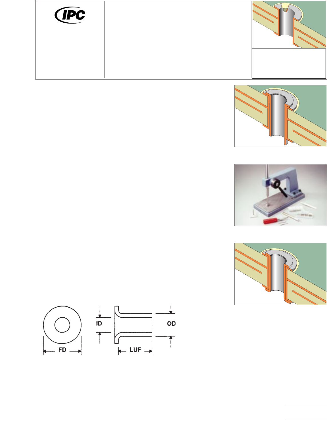
ID Inside Diameter
The eyelet inside diameter should be a 0.075 - 0.500 mm greater than the compo-
nent lead diameter.
LUF Length Under Flange
The length of the eyelet barrel under the flange should be 0.630 - 0.890 mm greater
than the thickness of the PC board. This added length allows for proper protrusion
when setting the eyelet.
FD Flange Diameter
The eyelet flange diameter should be small enough to prevent interference with adja-
cent pads or circuits.
OD Outside Diameter
The clearance hole should allow the eyelet to be inserted without force but should
not exceed 0.125 mm greater than the eyelet outside diameter.
NOTE
Be sure to select an eyelet meeting the proper criteria. An eyelet with an oversize
flange may interfere with adjacent circuits. An eyelet that is too short will not protrude
through the PC board for proper setting.
PROCEDURE
1. Clean the area.
2. Examine the hole to ensure that there is no damage to the wall of the hole.
Check continuity to establish the integrity of the connection.
3. Select an eyelet using the Eyelet Selection Criteria. Use a pin gauge and caliper
to measure the existing plated hole dimensions. The eyelet must have an inside
diameter sufficient to receive the component lead and an outside diameter that
will allow the eyelet to be inserted into the hole without force.
4. Remove oxides from the surface pads where the eyelet is to be installed using
a buffer and clean.
5. Apply a small amount of liquid flux to the pad or circuit on the PC board sur-
face, if any, and tin with solder using a soldering iron and solder. Clean the area.
6. Insert the eyelet into the hole. If a new circuit is required, the new circuit may
extend into the hole and the flange of the eyelet will secure the new circuit in
place. (See Figure 1.)
7. Select the proper setting tools and insert them into an eyelet press system. (See
Figure 2.)
8. Turn the PC board over and rest the eyelet flange on the lower setting tool.
9. Apply firm even pressure to form the eyelet barrel.
10. Apply a small amount of liquid flux and solder the eyelet flanges to the pads on
the PC board surface if necessary. Clean the area. Inspect for good solder flow
and wetting around the eyelet flanges and lands.
11. Clean the area.
12. Install the component lead and solder, if required.
IPC-7721A
Number: 5.2
Revision:
Date: 2/98
Subject: Plated Hole Repair, Double Wall Method
Page2of4
Copyright Association Connecting Electronics Industries
Provided by IHS under license with IPC
Not for Resale
No reproduction or networking permitted without license from IHS
--``,``,-`-`,,`,,`,`,,`---