IPC-4556 印制板化学镍钯浸金(ENEPIG)规范ENG.pdf - 第33页
APPENDIX 4 Factors Affecting Measurement Accuracy of ENEPIG Coatings by XRF Frank Ferrandino, T echnical Manager Calmetrics Inc. XRF has become ubiquitous in the plating industry for measuring plated layer thicknesses. A…
SUMMARY
• Based on the round robin testing, there should be concern regarding accuracy of ENEPIG measurements. If the protocols
outlined in the XRF APPENDIX 4 are not followed, then some equipment will at best be a random number generator.
• It is imperative that Gauge Repeatability & Reproducibility protocols be run on all XRF equipment used in the supply
chain and comparison testing using traceable certified national standards to ensure accuracy of measurement and hence
performance of the ENEPIG deposit.
• Some equipment currently in use for other surface finishes will not meet the requirements for accuracy and repeatability
and will need to be replaced - this is the cost of supplying and using ENEPIG as a multifunctional surface finish.
• Feature size affects the deposit thickness for ENEPIG similar to other finishes. The use of the specified 60 mil X 60 mil
pads cannot be emphasized enough to minimize variation between measurements that will make meeting the proposed
specification limits nearly impossible.
• The XRF supplier base was absent from the study and their lack of participation in correctly setting up, evaluating equip-
ment and suggesting alternatives for older equipment is troubling, to say the least. Without their support, ENEPIG perfor-
mance will be open to criticism that is not warranted, due to incorrect thicknesses being supplied.
IPC-4556-A3-5
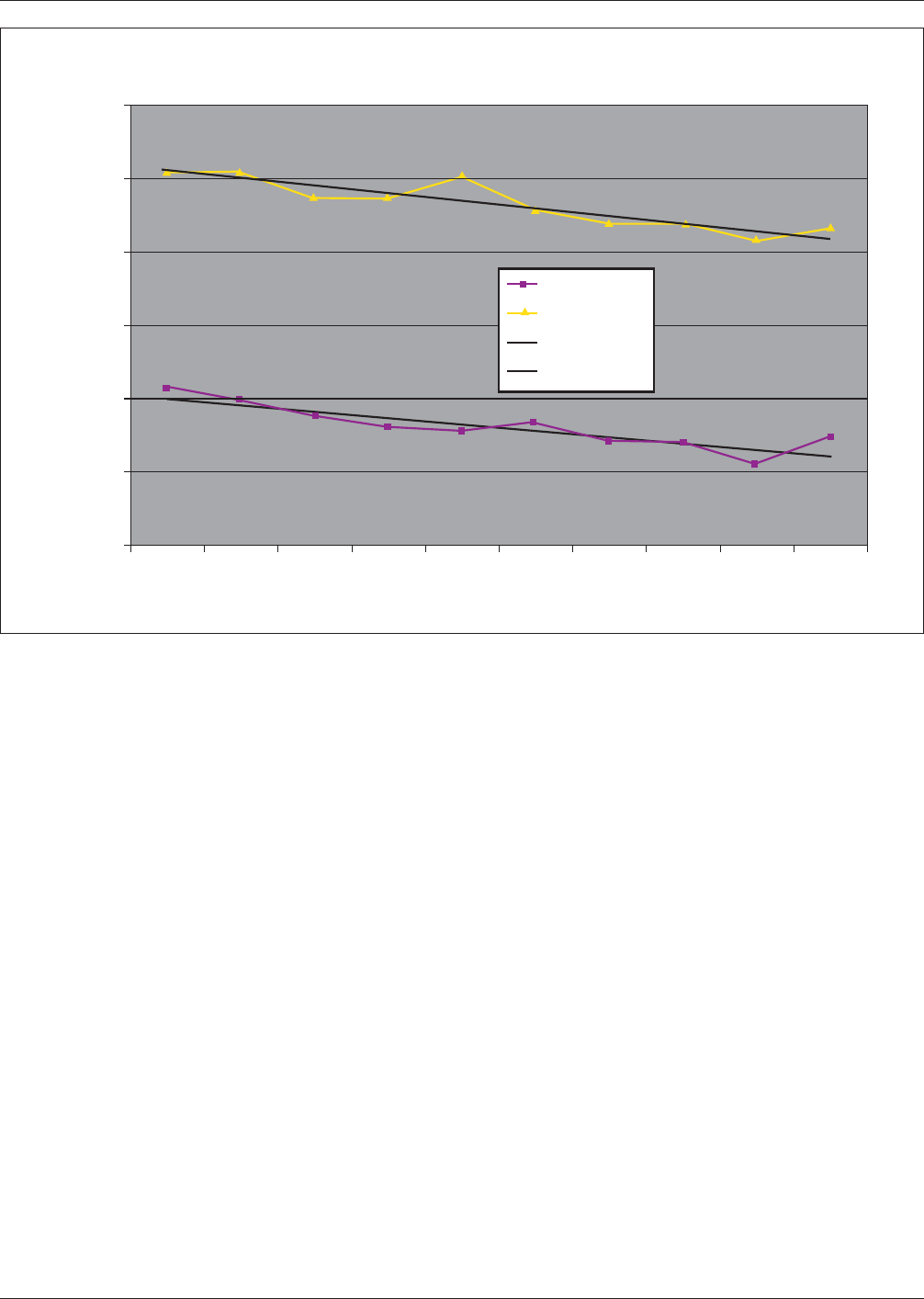
Figure A3-5 The Impact of Feature Size on Electroless Palladium and Immersion Gold Deposition Thickness Plated
on the Same PB
microinches
Au & Pd thickness as a function of pad area
380 380 452 452 612 612 1792 1792 50343 50343
area in mils square
y=-0.2012x+10.443
R
2
= 0.8099
y=-0.1752x+4.2373
R
2
= 0.7856
Au
Pd
Linear (Au)
Linear (Pd)
IPC-4556 January 2013
22

APPENDIX 4
Factors Affecting Measurement Accuracy
of ENEPIG Coatings by XRF
Frank Ferrandino, Technical Manager
Calmetrics Inc.
XRF has become ubiquitous in the plating industry for measuring plated layer thicknesses.
Among its many virtues, the XRF method tends to typically be robust for a wide range of plating applications. However,
the plating industry in response to increasing demand for reliability, continues to develop new coating combinations that can
make the analysis of thickness by XRF more complicated and therefore increasingly subject to error if not calibrated and
used properly. In particular, the use of ENEPIG coatings in the PCB industry, to improve shelf life and solderability, pres-
ent some challenges to the typical XRF instrument used to measure it.
Typical XRF Instruments Used for Plating Thickness Measurements A sizable majority of the XRF instruments used by
PCB manufacturers are good general purpose plating thickness testers equipped with either a tungsten (W) target or molyb-
denum (Mo) target x-ray source and gas filled proportional detectors. Such products are capable of achieving reasonably
good accuracy when measuring ENEPIG plating thicknesses. On the other hand, it is also easy for measurement accuracy to
be compromised when such XRF instruments do not have certain software functions or are not properly calibrated.
Below is a list of potential sources of errors when measuring ENEPIG coatings with proportional counter XRF systems using
W or Mo x-ray sources:
(1) The PCB epoxy laminate often contains fire retardant compounds of bromine.
The default measurement condition for these types of XRF instruments is to count the number of Au x-rays detected for
the Au L-β line (energy ~ 11.4 keV).
This is because the Au L-α peak overlaps the Cu x-ray peaks which originate from the Cu layer. In XRF analysis, we
try to avoid interferences caused by such overlaps when possible, hence the usual choice of analyzing the Au L-β line.
Normally when plating on Cu or Cu alloy substrates there is no interference with the Au L-β peak. However, in the
case of PCB samples, there is a reasonably good chance that some Br x-ray emission will be detected from the epoxy
substrate. Given the relatively poor energy resolution of proportional counter x-ray detectors, Br, with a K-α energy of
~ 11.9 keV will produce a spectral peak that overlaps or interferes with the usually reliable Au L-β peak. Normally, Br
x-ray intensity will be low since the Br x-rays must pass through the Cu, Ni, Pd, and Au layers to reach the detector
and be counted. These layers provide significant reduction in Br intensity due to shielding, resulting in only a small,
minor Br peak intensity.
In the case of immersion Au layers, which only produce a low intensity Au L-β peak, this small Br contribution to the
peak intensity of Au, if not corrected, can be significant since the Br contribution to the Au peak intensity is roughly
the same level of magnitude or even greater compared to the Au peak intensity itself.
When measuring immersion Au layers in the 0.05 µm - 0.13 µm [2 - 5 microinch] range uncorrected Br interference can
add anywhere from a few sub-microns or microinches for the gold measurements to as much as tenths of microns or
tens of microinches. Therefore, a Au layer which is truly 0.1 micron [4 microinches] for example, may measure any-
where from 0.15 µin to 0.25 µm [6 µin to 10 µin ] or more, if the Br interference is not accounted for and corrected.
The amount of error will depend primarily on the thickness of the Cu layer (thinner copper results in larger errors in
an Au measurement), the amount of Br compound in the epoxy and the spatial resolution of the x-ray beam and its
position relative to the plated areas being measured.
Fortunately, most if not all the XRF instruments used for plating thickness measurements offer peak deconvolution soft-
ware. This software will allow the instrument to breakdown the composite Au + Br peak into its component parts.
Therefore, it is possible to extract Au L-β peak intensity information independent of the contributing interference from
Br. For accurate measurement of immersion Au on PCB’s, use of a peak deconvolution routine is prudent and in many
cases absolutely vital to maximizing the accuracy of the Au thickness measurement. It should be noted that significant
errors in Au thickness measurement due to uncorrected Br interference will contribute to errors in the calculation of
underlying electroless Ni and Pd thicknesses, as well.
January 2013 IPC-4556
23

(2) A second source of potential error lies with the electroless nickel layer. Proportional counter based XRF instruments
cannot measure phosphorous content in the Ni layer directly. Therefore it is generally assumed in the calibration of the
instrument that the Ni layer contains some constant amount of phosphorous composition, typically about 8%. However,
if the sample does not contain 8% phosphorous in the Ni layer, errors in electroless Ni thickness will occur. As a very
rough rule of thumb, one can expect about a 4% thickness error for each 1% difference in phosphorous content between
the sample under test and the standards used for calibration.
The electroless nickel thickness measurement will be erroneously high if the sample phosphorous content is less than
the calibration standard. The measurement of thickness will be erroneously low if the sample contains more phospho-
rous than the standards used for calibration. Since most platers maintain the phosphorous content at approximately 8%,
the electroless nickel thickness measurement error is normally minor.
Although electroless Ni thickness errors due to phosphorous content variations are normally less than 10%, it is pos-
sible to correct for changes in sample phosphorous content if they are known. Some XRF software does offer such cor-
rections which allow the user to enter the known % P content in the nickel layer and the thickness measurement will
automatically be corrected. Alternatively, suppliers of such XRF instrumentation should be able to provide correction
factors for changes in sample % P which can be entered as ‘‘density’’ factors that can correctly compensate for changes
in sample % P.
(3) Measurement of the immersion Pd layer is subject to two possible errors. The more significant potential error is caused
by variations in the x-ray background level in the spectral region where the Pd K-α peak is detected. The Pd K-α peak
is added to this background level. Typically, XRF plating thickness measuring instruments integrate this area to obtain
Pd intensity and relate that intensity to Pd thickness. In the case of immersion Pd where thicknesses are in the order of
0.05 µm - 0.15 µm [2 µin - 6 µin], the spectrum background level is often as intense or more intense than the Pd peak
itself. If the background level is constant, this influence may be included in the calibration. However, the background
level may, in fact, vary. This potential background level variation is a function mainly of the Cu layer’s thickness below
the Pd.
The background scatter originates mainly from the epoxy substrate. The W or Mo target x-ray sources provide a broad
band of x-ray energies to the sample during the measurement. It is mainly the higher energy x-rays that will penetrate
the thick Cu-clad laminate, scatter back from the epoxy through the Cu layer to be detected and seen in the measured
spectrum. Lower energy x-rays originating from the source, do not have enough energy to penetrate the Cu layer twice
and be detected. Therefore background ‘‘noise’’ is only an issue in the higher end of the x-ray energy spectrum.
It is in this high end of the spectrum that the Pd K-α appears (~ 21.1 keV). The amount of background scatter that
reaches the detector is again a function of the Cu thickness since the scattered x-rays are shielded primarily by this rela-
tively thick layer. As with the Br interference with Au, the background scatter will be a function of the underlying Cu
thickness as well as the spatial resolution of the x-ray beam and the position of the beam relative to the edges of the
sample plated area.
Again, to be prudent and to optimize accuracy of Pd thickness measurements, the potential varying background level
should be compensated for to obtain net Pd intensity information. Most XRF instruments are equipped with background
correction software to deal with this issue and obtain reasonably accurate net Pd intensities. The user should be famil-
iar with how to access this feature if its use is optional, or know if automatic background correction is always used by
their XRF instrument to measure plating thickness. There are a wide variety of background correction schemes that are
available, some of which are more effective in this case than others.
Other approaches to mitigate Pd measurement errors due to varying background levels include the use of primary beam
filters to attempt to suppress the background level to a magnitude far below that of the Pd K-α peak intensity. This
method can work well when using, for example, a Mo filter with a larger collimator. Since primary filters reduce over-
all signal intensity the filter material and thickness must be selected with an attempt to balance the gains from reduc-
ing the background and the loss due to reduced Pd signal intensity. Typically, primary filters are effective only when
using larger x-ray beam collimators. Users should consult with the manufacturer of the instrument before attempting to
use a primary filter.
Less significantly for the commonly used XRF instrument is the error bias that may be introduced by the fact that
immersion Pd layers are not pure Pd. Instead, it is common that such layers contain about 2% phosphorous. Like the
electroless nickel measurement, the level of phosphorous in the plating has some effect on the thickness measurement.
IPC-4556 January 2013
24