IPC-4556 印制板化学镍钯浸金(ENEPIG)规范ENG.pdf - 第80页
The metric of solderability was the contact angle, θ c . The lower the contact angle, the better is the solderability . The value of θ c was determined by the combination of two test methods. The first method is the menis…

APPENDIX 11
Solderability Testing Helps Select Surface Finishes
E. P. Lopez and P. T. Vianco
Sandia National Laboratories
1
AWS Feature Article
INTRODUCTION
New surface finishes are being sought by both structural and electronics market places to improve the solderability of com-
mon and advanced base materials as well as to address environmental regulations that restrict the use of lead (Pb). Ideally,
any new surface finish would be compatible with either conventional Sn-Pb or Pb-free solder applications. It is necessary
to test the solderability behavior of these alternative finishes prior to their use on materials for assembly operations. One
such surface finish that is currently capturing industry interest is Electroless Nickel (Ni)-Electroless Palladium (Pd)-
Immersion Gold (Au) or ENEPIG. In this layer stack, the Ni layer is the solderable finish to which the solder joint is actu-
ally formed at the completion of the soldering process. The Pd layer is a protective finish to maintain the solderability of
the Ni layer. The thin Au layer is a protective finish, as well, maintaining the solderability of the Pd layer because the lat-
ter forms a very thin oxide layer that slows the wetting and spreading of tin (Sn)-based solders.
The ENEPIG finish improves upon the good solderability of the original electroless nickel-immersion gold (ENIG), but with
two benefits provided by the Pd addition. First, Pd eliminates the black pad solder joint defect [1]. The term ‘‘Black Pad’’
was first used in the late ’90s to describe a specific kind of nickel corrosion on ENIG surface finish. This corroded nickel
compromises the solderability of the part. In cross sections of the failed joint, Ni
3
Sn
4
(for Sn-Pb solder joints) or (Cu,Ni)
6
Sn
5
(for SAC alloy solder joints) intermetallic (IMC) is found on the solder side, and a phosphorous (P) content higher than that
of the bulk Ni(P) plating is detected on the pad side [1]. Secondly, Pd slows the diffusion of Ni into the Au layer, resulting
in longer shelf life and higher reliability for printed wiring assemblies exposed to harsh operating environments.
Experimental/Discussion In the study reported here, the solderability of the ENEPIG finish was evaluated on oxygen-free-
electronic (OFE) grade copper (Cu) coupons. The coupons were tested in the as-fabricated condition and after exposure to
two accelerated storage environments. The two accelerated storage environments included: (1) exposure to a Battelle Class
2 environment and (2) steam aging per ANSI J-STD-002C ‘‘Solderability Tests for Component Leads, Terminations, Lugs,
Terminals, and Wire’’ (2007) [2]. The Battelle Class 2 test is a mixed flowing gas test containing 10 ppb H
2
S; 200 ppb NO
2
;
10 ppb Cl
2
; 70% relative humidity (RH); at 30 °C. The Battelle Class 2 accelerated environment was selected because it
represents long-term storage under the conditions of a light industrial/manufacturing environment [2]. The length of the
Class 2 accelerated aging test represents the equivalent of 3 months to 10 years for contact materials such as copper and
silver. As such, the test is designed to accentuate plating defects. Steam aged test coupons were exposed for 8 and 24 hours
within an atmosphere of 90% RH and temperature of 85 °C. For brevity, the discussion below will focus only on the sol-
derability behavior after exposure to the Battelle Class 2 environment.
The ENEPIG finish was obtained from two vendors denoted ‘‘1’’ and ‘‘2.’’ Copper coupons plated by Vendor 1 had nominal
layer thicknesses shown below:
Vendor 1:
1. 150-180 µin Ni, 6-7 µin Pd and 2-3 µin Au.
The second supplier, Vendor 2, provided two variants of the ENEPIG finish with the following thicknesses:
Vendor 2:
1. 150-180 µin Ni, 6-7 µin Pd and 2-3 µin Au
2. 150-180 µin Ni, 2-4 µin Pd and 2-3 µin Au.
The difference between the two Vendor 2 variants was the thickness of the Pd layer:6-7µin(‘‘thick’’)and2-4µin
(‘‘thin’’). A thin Pd layer reduces the material cost of the ENEPIG finish; however, the potential tradeoff is a reduced bar-
rier function between the Ni and Au layers. The solderability of the test specimens was evaluated using a rosin-based, mildly
activated (RMA) flux with a eutectic 63Sn-37Pb (wt.%) solder. The solder bath was held at 245 °C.
1. Sandia is a multi-program laboratory operated by Sandia Corporation, a Lockheed Martin Company, for the United States Department of Energy’s National
Nuclear Security Administration under Contract DE-AC04-94AL85000.
January 2013 IPC-4556
69
The metric of solderability was the contact angle, θ
c
. The lower the contact angle, the better is the solderability. The value
of θ
c
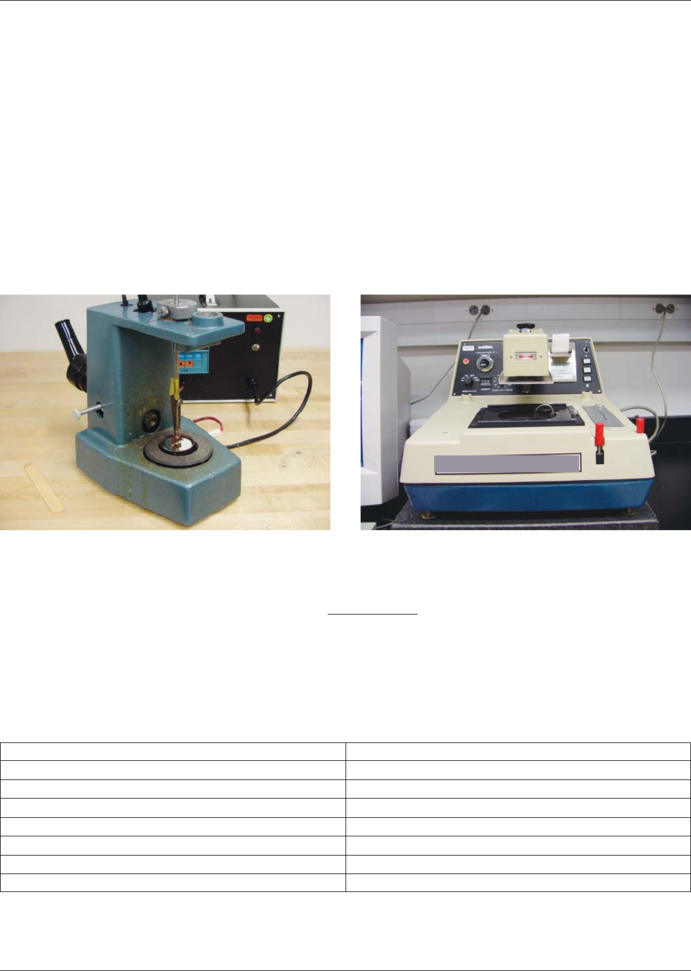
was determined by the combination of two test methods. The first method is the meniscometer test. This test measures
the meniscus height, H, or vertical movement of a solder meniscus up the side of the coupon, using a traveling microscope
(Figure A11-1a). Five trials were performed per each test condition. A mean value for H and standard deviation were deter-
mined from those tests.
The second test method utilized a wetting balance (Figure A11-1b) to measure the weight of the meniscus that forms on the
coupon. Five separate tests were performed with this technique. The meniscus weight was described by the mean of those
five values and one standard deviation. When the flux-coated coupon is immersed into a solder bath, initially an upward
force is exerted on the sample. The upward force is caused by (a) the solder displaced by the sample volume plus (b) the
solder that is displaced by the nonwetting or ‘‘negative’’ meniscus prior to the start of the wetting action. As wetting and
spreading of the molten solder progresses up the coupon, the negative meniscus is lost, and the solder then generates a down-
ward force because of its weight. However, the buoyancy force is not lost; it remains pushing up on the coupon and, as
such, must be taken into account when calculating the net force or weight, w, of the molten solder meniscus on the coupon.
Once these measurements have been obtained, the value of θ
C
, is calculated using Equation 1, where ρ is the solder den-
sity, g is the acceleration due to gravity, P is the sample perimeter (cm), and H is the meniscus height.
θ
c
= sin
−1
[
4
2
w −
(
pgPH
2
2
4w
2
+
(
)
pgPH
2
)
2
]
Equation 1
In general, solderability is considered good-to-excellent for electronic and structural applications when the value of θ
C
is
less than 30 °. Solderability is adequate as long as θ
C
remains less than 50 ° as has been validated by the use of Pb-free
solders on printed wiring assemblies [3,4,5,6]. A more inclusive guideline is shown in Table A11-1 [7].
Figure A11-1a Meniscometer Figure A11-1b Wetting Balance
Table A11-1 ‘‘Relative Wettability Guideline,’’ Using Contact Angle (θ
C
) As ‘‘General’’ Metric
Relative Wettability Contact Angle (θ
C) Range
Perfect 0° < θ
C
<10°
Excellent 10° < θ
C
<20°
Very Good 20° < θ
C
<30°
Good 30° < θ
C
<40°
Adequate 40° < θ
C
<50°
Poor 55° < θ
C
<70°
Very Poor 70° < θ
C
IPC-4556 January 2013
70
MULTICORE SOLDERS

A second parameter that is obtained from the wetting balance test is the wetting rate. The wetting rate indicates the speed
with which the molten solder meniscus climbs the coupon.
Although this parameter is not used within industry standards, testing at Sandia National Laboratories has determined that
it provides a correlation between the laboratory test and performance in fielded processes.
Test Results - Contact Angle, θ
C
The contact angle data for Vendors 1 and 2 are plotted in Figure A11-2 as a function of
the exposure time in the Battelle Class 2 environment. If the actual storage environment is a Class 2 environment, the fol-
lowing correlation between the accelerated test exposure time and the actual storage lifetimes is as follows:
• 8.4 hrs corresponds to ~ 3 months;
• 33.6 hrs,~1yr;
• 168 hrs, ~ 5 yrs; and
• 336 hrs, ~ 10 yrs.
It is clear that, the ENEPIG finishes, used in conjunction with the Sn-Pb solder and RMA flux, exhibited excellent solder-
ability that was not degraded by even the longest exposure to the Class 2 conditions. In fact, the contact angles of the Ven-
dor 1 finish actually decreased slightly after exposure to the Battelle Class 2 conditions. Although both ‘‘thick’’ and ‘‘thin’’
variants from Vendor 2 have only been aged for 168 hours (~ 5 yrs), the contact angles remained very low and unaffected
by the Class 2 exposure. More importantly, it is also apparent that the two Pd thicknesses of these ENEPIG finishes pro-
vided comparable solderability performances, which opens the door to using the less-expensive, thinner Pd layer.
IPC-4556-a11-2
Figure A11-2 ENEPIG with Thin and Thick Pd from Vendors1&2–Contact angles as a function of Battelle Class 2 aging using
Sn63Pb37 solder, RMA flux and 245 °C max. temperatures.
0
5
10
15
20
25
30
35
40
ENEPIG Sn63-Pb37
245C
Contact Angle Vendor 1 Thick Pd
Contact Angle Vendor 2 Thin Pd
Contact Angle Vendor 2 Thick Pd
Aging Time (hrs)
Contacr Angle (º)
January 2013 IPC-4556
71