IPC-4556 印制板化学镍钯浸金(ENEPIG)规范ENG.pdf - 第78页
25 23 21 19 17 15 13 11 9 7 5 3 1 50 40 30 30 A u [n Ob s erv a t i o n m] Ref LS L + 4 . 0 * S t D e v R epo rted by : LS L: 2 5 Ref er en c e 49 Me a n 4 8 . 9 2 S tD ev 0.286 6 * S tD ev ( S V ) 1.718 LS L 2 5 B a si …
Typical Measurement data achievable with properly calibrated SDD-Detector XRF
Nominal values of standard measured, Au49nm/Pd100nm/Ni4387nm
N Au [nm] Pd [nm] Ni [nm]
1 48.5 97.9 4375
2 48.7 98.6 4381
3 48.6 99.0 4383
4 48.8 100.1 4392
5 49.0 100.1 4388
6 48.8 100.0 4394
7 48.8 99.8 4385
8 48.8 98.9 4384
9 48.9 99.3 4383
10 49.3 100.4 4390
11 48.9 99.7 4385
12 49.2 100.7 4389
13 49.0 101.0 4393
14 49.4 99.7 4390
15 48.8 99.7 4396
16 49.2 100.7 4394
17 48.6 99.6 4387
18 48.9 100.3 4387
19 49.1 100.2 4386
20 49.1 100.4 4395
21 49.3 100.5 4390
22 48.5 100.0 4395
23 48.4 99.0 4383
24 49.2 98.5 4389
25 49.1 98.0 4385
Mean 48.92 nm 99.68 nm 4388.0 nm
Standard Deviation 0.286 nm 0.837 nm 5.112 nm
C.O.V. (%) 0.59 0.84 0.12
Range 1.07 nm 3.14 nm 20.2 nm
# of readings 25 25 25
Min. Read. 48.4 nm 97.9 nm 4375 nm
Max. Read. 49.4 nm 101.0 nm 4396 nm
Measuring Time 120 sec 120 sec. 120 sec.
January 2013 IPC-4556
67
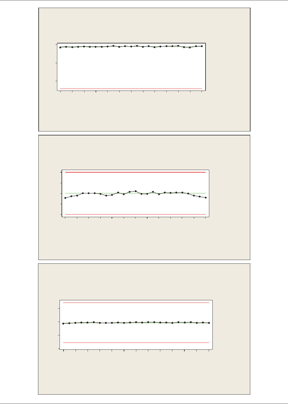
25
23
21191715131197531
50
40
30
30
A
u
[n
Observation
m]
Ref
LS L + 4.0 * S tD ev
Reported by :
LS L: 25
Reference 49
Mean 48.92
StDev 0.286
6 * S tDev (S V ) 1.718
LS L 25
Basic S tatistics
Misc: ENEPIG-Au Measurements
Type 1 Gage Study for Au
Gage name:XRF
Run Chart of A u
Date of study :
252321191715131197531
110
105
100
95
90
Observation
Pd
Ref
Ref + 0.10 * Tol
Ref - 0.10 * Tol
Basic S tatistics
Reference 100
Mean 99.68
6 * S tDev (S V ) 5.021
Tolerance (Tol) 100
StDev 0.837
C apability
C g 3.98
Cgk 3.86
Reported by :
Tolerance: 100
Gage name:XRF
% V ar(Repeatability ) 5.02%
% V ar(Repeatability and Bias) 5.19%
Date of study :
Misc: ENEPIG-Pd Measurements
Run Chart of Pd
Type 1 Gage Study for Pd
252321191715131197531
4600
4400
4200
4000
Observation
Ni
Ref
Ref + 0.10 * Tol
Ref - 0.10 * Tol
Basic S tatistics
Reference 4387
Mean 4388.02
6 * S tDev (S V ) 30.670
Tolerance (Tol) 3000
StDev 5.112
C apability
C g 19.56
C gk 19.50
Reported by :
Tolerance: 3000
Gage name:XRF
% V ar(Repeatability ) 1.02%
%V ar(Repeatability and Bias) 1.03%
Date of study :
Misc: ENEPIG-Ni Measurements
Run Chart of Ni
Type 1 Gage Study for N i
IPC-4556 January 2013
68

APPENDIX 11
Solderability Testing Helps Select Surface Finishes
E. P. Lopez and P. T. Vianco
Sandia National Laboratories
1
AWS Feature Article
INTRODUCTION
New surface finishes are being sought by both structural and electronics market places to improve the solderability of com-
mon and advanced base materials as well as to address environmental regulations that restrict the use of lead (Pb). Ideally,
any new surface finish would be compatible with either conventional Sn-Pb or Pb-free solder applications. It is necessary
to test the solderability behavior of these alternative finishes prior to their use on materials for assembly operations. One
such surface finish that is currently capturing industry interest is Electroless Nickel (Ni)-Electroless Palladium (Pd)-
Immersion Gold (Au) or ENEPIG. In this layer stack, the Ni layer is the solderable finish to which the solder joint is actu-
ally formed at the completion of the soldering process. The Pd layer is a protective finish to maintain the solderability of
the Ni layer. The thin Au layer is a protective finish, as well, maintaining the solderability of the Pd layer because the lat-
ter forms a very thin oxide layer that slows the wetting and spreading of tin (Sn)-based solders.
The ENEPIG finish improves upon the good solderability of the original electroless nickel-immersion gold (ENIG), but with
two benefits provided by the Pd addition. First, Pd eliminates the black pad solder joint defect [1]. The term ‘‘Black Pad’’
was first used in the late ’90s to describe a specific kind of nickel corrosion on ENIG surface finish. This corroded nickel
compromises the solderability of the part. In cross sections of the failed joint, Ni
3
Sn
4
(for Sn-Pb solder joints) or (Cu,Ni)
6
Sn
5
(for SAC alloy solder joints) intermetallic (IMC) is found on the solder side, and a phosphorous (P) content higher than that
of the bulk Ni(P) plating is detected on the pad side [1]. Secondly, Pd slows the diffusion of Ni into the Au layer, resulting
in longer shelf life and higher reliability for printed wiring assemblies exposed to harsh operating environments.
Experimental/Discussion In the study reported here, the solderability of the ENEPIG finish was evaluated on oxygen-free-
electronic (OFE) grade copper (Cu) coupons. The coupons were tested in the as-fabricated condition and after exposure to
two accelerated storage environments. The two accelerated storage environments included: (1) exposure to a Battelle Class
2 environment and (2) steam aging per ANSI J-STD-002C ‘‘Solderability Tests for Component Leads, Terminations, Lugs,
Terminals, and Wire’’ (2007) [2]. The Battelle Class 2 test is a mixed flowing gas test containing 10 ppb H
2
S; 200 ppb NO
2
;
10 ppb Cl
2
; 70% relative humidity (RH); at 30 °C. The Battelle Class 2 accelerated environment was selected because it
represents long-term storage under the conditions of a light industrial/manufacturing environment [2]. The length of the
Class 2 accelerated aging test represents the equivalent of 3 months to 10 years for contact materials such as copper and
silver. As such, the test is designed to accentuate plating defects. Steam aged test coupons were exposed for 8 and 24 hours
within an atmosphere of 90% RH and temperature of 85 °C. For brevity, the discussion below will focus only on the sol-
derability behavior after exposure to the Battelle Class 2 environment.
The ENEPIG finish was obtained from two vendors denoted ‘‘1’’ and ‘‘2.’’ Copper coupons plated by Vendor 1 had nominal
layer thicknesses shown below:
Vendor 1:
1. 150-180 µin Ni, 6-7 µin Pd and 2-3 µin Au.
The second supplier, Vendor 2, provided two variants of the ENEPIG finish with the following thicknesses:
Vendor 2:
1. 150-180 µin Ni, 6-7 µin Pd and 2-3 µin Au
2. 150-180 µin Ni, 2-4 µin Pd and 2-3 µin Au.
The difference between the two Vendor 2 variants was the thickness of the Pd layer:6-7µin(‘‘thick’’)and2-4µin
(‘‘thin’’). A thin Pd layer reduces the material cost of the ENEPIG finish; however, the potential tradeoff is a reduced bar-
rier function between the Ni and Au layers. The solderability of the test specimens was evaluated using a rosin-based, mildly
activated (RMA) flux with a eutectic 63Sn-37Pb (wt.%) solder. The solder bath was held at 245 °C.
1. Sandia is a multi-program laboratory operated by Sandia Corporation, a Lockheed Martin Company, for the United States Department of Energy’s National
Nuclear Security Administration under Contract DE-AC04-94AL85000.
January 2013 IPC-4556
69