IPC-4556 印制板化学镍钯浸金(ENEPIG)规范ENG.pdf - 第54页
IPC-4556-a6-5 100 Figure A6-5 Solder Spread Results Using an ROL0 Pb-free Solder Paste of the SAC 300 Family on ENEPIG Deposits (Note: The ENEPIG deposits are from 7 dif ferent chemistry suppliers (with dif ferent electr…
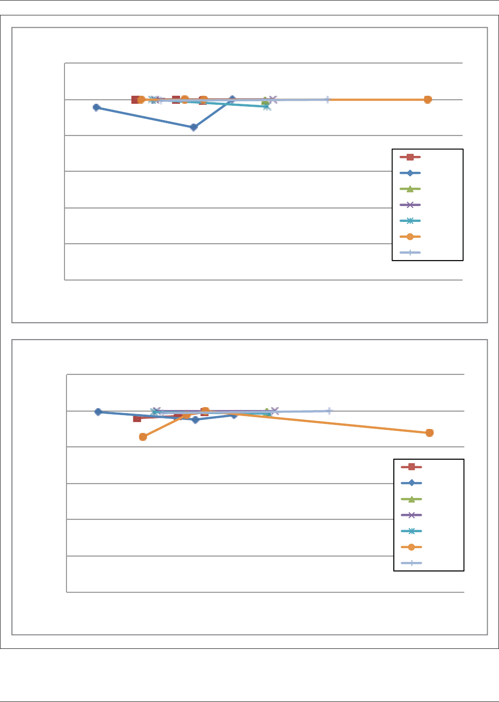
IPC-4556-a6-4
Figure A6-4 Solder Spread Results Using an ROL1 Sn/Pb/Ag Solder Paste on ENEPIG Deposits
(Note: The ENEPIG deposits are from 7 different chemistry suppliers (with different electroless palladium thicknesses) using the solder spread
pattern. The Figure A6-4 - Top is for boards as-received. The Figure A6-4 - Bottom is for soldering after pre-conditioning of the boards for 8
hours at 72 °C [162 °F] and 85% RH).
110%
110%
110%
80%
70%
60%
50%
Solder Spread (%
0.00 0.05 0.10 0.15 0.20 0.25 0.300.35 0.40 0.45 0.50
)
SnPb ROL1 – No Conditionin
Actual Pd Thickness (um)
g
Chem A
Chem B
Chem C
Chem D
Chem E
Chem F
Chem G
110%
110%
110%
80%
70%
60%
50%
Solder Spread (%
0.00 0.05 0.10 0.15 0.20 0.25 0.300.35 0.40 0.45 0.50
)
Actual Pd Thickness (um)
SnPb ROL1 – Post 72 C/85% RH
Chem A
Chem B
Chem C
Chem D
Chem E
Chem F
Chem G
January 2013 IPC-4556
43
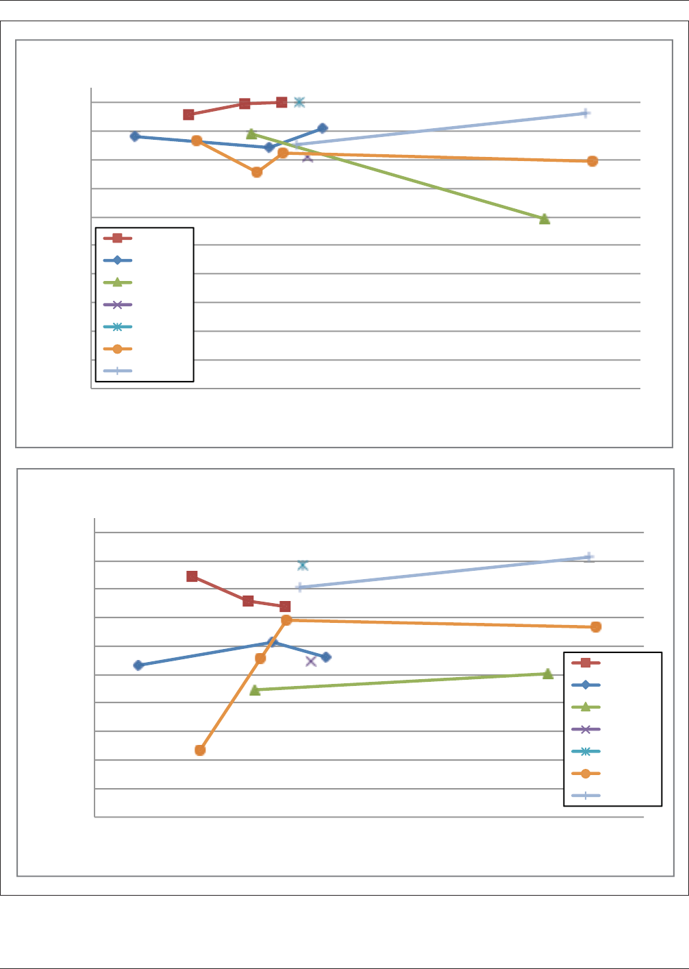
IPC-4556-a6-5
100
Figure A6-5 Solder Spread Results Using an ROL0 Pb-free Solder Paste of the SAC 300 Family on ENEPIG Deposits
(Note: The ENEPIG deposits are from 7 different chemistry suppliers (with different electroless palladium thicknesses) using the solder spread
pattern. The Figure A6-5 - Top is for boards as-received. The Figure A6-5 - Bottom is for soldering after pre-conditioning the boards for 8 hours
at 72 °C [162 °F] and 85% RH).
%
90%
80%
70%
60%
50%
40%
30%
20%
10%
0%
Solder Spread (%
0.00 0.05 0.10 0.15 0.20 0.25 0.300.35 0.40 0.45 0.50
)
Actual Pd Thickness (um)
100%
90%
80%
70%
60%
50%
40%
30%
20%
10%
0%
Solder S
pread (%
0.00 0.05 0.10 0.15 0.20 0.25 0.300.35 0.40 0.45 0.50
)
Actual Pd Thickness (um)
PB-free ROL0 – No Condioning
Chem A
Chem B
Chem C
Chem D
Chem E
Chem F
Chem G
Pb-free ROL0 – Post 72 C/85% RH
Chem A
Chem B
Chem C
Chem D
Chem E
Chem F
Chem G
IPC-4556 January 2013
44
Pb-Free Soldering The solder spread results using a Pb-free solder paste (ROL0) showed more variation between the dif-
ferent ENEPIG suppliers. For boards just out of the package (no pre-conditioning), solder spread values ranged from
60-100%. The differentiation between ENEPIG deposits is interesting, and may indicate some differences between the pro-
cess chemistries, but 60% would still be considered ‘good’ solder spread. For comparison, past measurements of OSP mate-
rials with the same solder paste achieved ~ 20% spread with no pre-conditioning. Note: A high spread value may not be
necessary to achieve an acceptable solder joint, depending on the situation (pad, stencil aperture, component, etc.).
There was a negative impact to the solder spread from the damp heat pre-conditioning (8 hours, 72 °C [162 °F]/85% RH) on
the ENEPIG deposits for the Pb-free solder paste and reflow. For samples with the same ENEPIG chemistry and target elec-
troless palladium thickness, the solder spread for the damp heat conditioned sample was lower every time. As seen in Figure
A6-5, solder spread percentages on some ENEPIG samples after damp heat dropped to values as low as 24%, while others
achieved spreads near 90%.
Industry pass/fail criteria are not yet established for the solder spread test. The 24% spread value represents an average
spread over 16 spread coupons (96 lines); within this board, some individual lines had very low spread, which is indicative
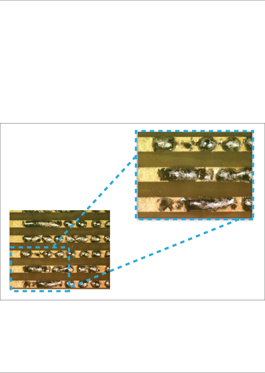
of high wetting angles and possibly localized dewetting. Figure A6-6 confirms the localized dewetting, as some solder depos-
its after coalescing, can be seen to have pulled back from their original deposit positions along the trace.
Using XRF data collected for samples from the same batches (not the exact same boards used for spread testing), the sol-
der spread results were plotted against measured immersion gold (IG), electroless palladium (EP) and electroless nickel (EN)
layer thicknesses. No correlation was found between the achieved solder spread and the IG or EP thicknesses (all R
2
val-
ues were less than 0.1). The EN layer thicknesses, however, did show a relationship to the solder spread results (see Figure
A6-7). Thicker layers of EN resulted in the highest solder spread results with the Pb-free solder paste. The lowest Pb-free
spread results were observed for the thinnest EN layers - this effect was most apparent for the damp heat conditioned
samples.
IPC-4556-a6-6
Figure A6-6 Solder Spread for Lowest Spread ENEPIG Sample Showing Evidence of High Contact Angle and Dewetting for
Some Areas of the Printed Board
January 2013 IPC-4556
45