allied-catalog-2013.pdf - 第58页
58 (800) 675-1 1 18 (USA & Canada) (310) 635-2466 (Worldwide) Milling X-Prep ® Applications 3D TSV – Stacked Die ● Flip-chip - GPU ● NAND/Flash memory ● SoC, PoP and SiC – mobile processors ● Hybrid Super SoC’s ● WL/…

57
www.alliedhightech.com
Milling
Item Description
3D capability is required to uniformly deprocess
warped samples exhibiting either a convex or
concave physical profile. It is useful for package
deprocessing and die thinning for electrical fault
localization methods that demand extreme
uniformity of material removal and final thickness
control.
The advantage of deprocessing a device by
following its physical profile is that it remains in its
“as-manufactured” physical state. This approach
increases accuracy of material removal and
reduces the risk of either mechanically induced or
post-processing stress relaxation damage such as
cracking or delamination.
The 3D software module supports the use and/or
creation of custom/predictive maps to control the
milling profile. Both symmetrical and asymmetrical
profiles can be used and adjusted to match the
physical changes encountered, providing a high
degree of versatility to the operator.
● Stacked die deprocessing – X-ray image
before (top) and after (bottom)
● 8-layer die stack deprocessed to die 7
● 4-layer board deprocessed to layer 1
Convex/curved die profile
Flat plane deprocessing produces nonuniform
material removal and thickness.
Deprocessing the device by following its profile
ensures uniform material removal.
Ultrathin Die Deprocessing
Uniform
FR4 substrate
delayering
Uniform flip-chip
silicon thinning
In support of:
Package-level failure analysis
TDR, GMR/SQUID & Lock-In Thermography
Laser/Photon EFA Tools
● High NA SIL
High-Throughput FIB processing
● Design debug/circuit edit
Nano/e-Probing
3D Deprocessing
15-9171 3D Software Module
58
(800) 675-1118 (USA & Canada) (310) 635-2466 (Worldwide)
Milling
X-Prep
®
Applications
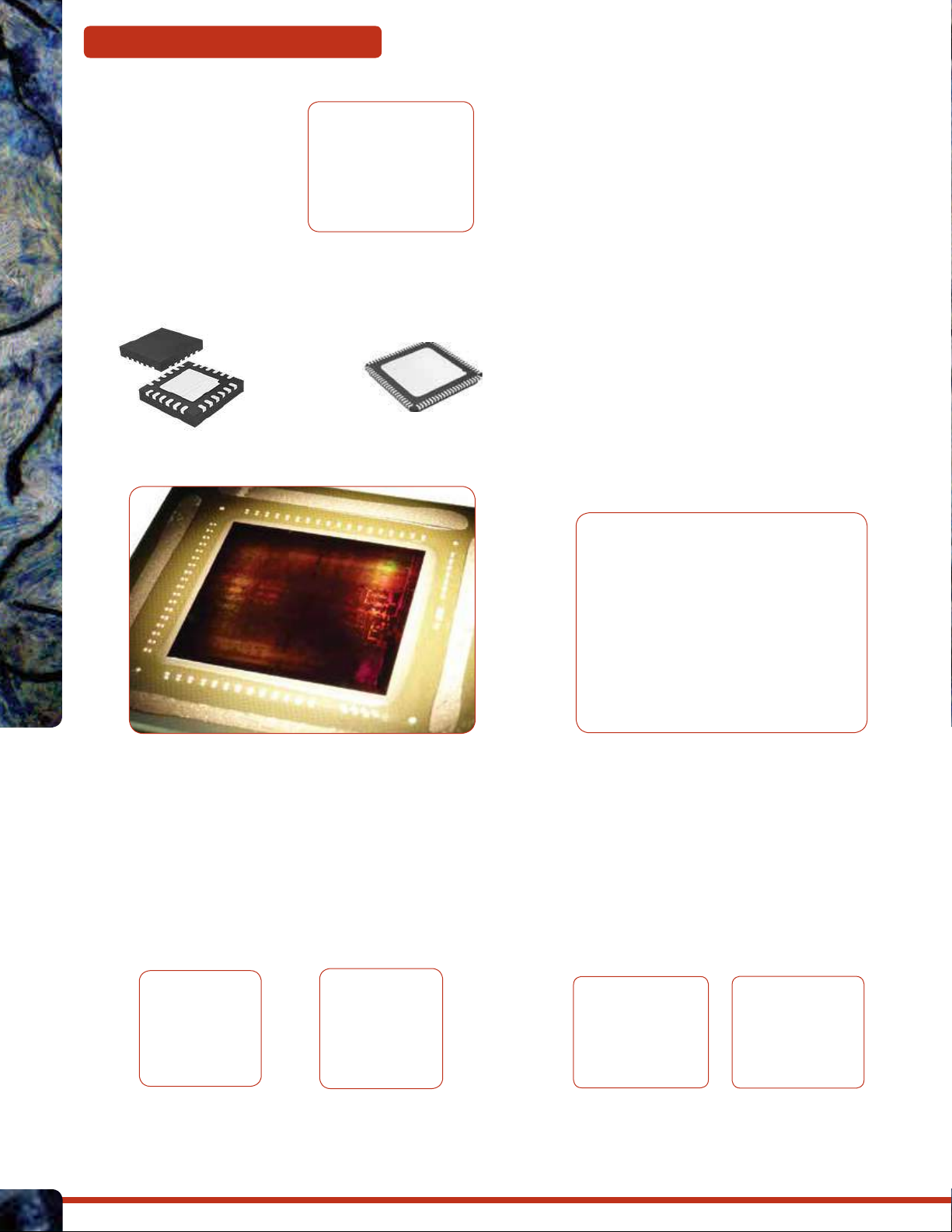
3D TSV – Stacked Die
● Flip-chip - GPU
● NAND/Flash memory
● SoC, PoP and SiC – mobile processors
● Hybrid Super SoC’s
● WL/CSP – Wafer and chip-scale package
● 2.5D Devices - FPGA
Lead Frame
● Thin small outline package (TSOP)
● Shrink small outline package (SSOP)
● Small outline IC (SOIC)
● Dual inline package (DIP)
Leadless Quad
● Plastic leaded chip carrier (PLCC)
● Quad flat no-lead (QFN)
● Quad flat package (QFP)
Silicon die thinned to near transparency through the backside
Pre-chemical decapsulation - Cu bond wire
MOSFET/Bipolar device FA
Small device deprocessing
MCMQFN
Ceramic package
Uniform copper (Cu) pillar
deprocessing - molded
package, stacked die
Uniform ultrathin
bare die silicon
thinning

59
www.alliedhightech.com
Milling
Single-point measurement display
X-Prep
®
Vision
™
Substrate Measurement Instrument
Features:
Multipoint scan or single-point thickness
measurement
10 µm to 1 mm thick range of measurement
(15 nm to 1 mm thick when configured with
#15-51000 Spectrometer)
Motorized, automatic X/Y/Z with autofocus and
< 1s acquisition time
"Drive to Coordinate" software navigation
Viewing of either 2D plot/map or 3D graph
Software automation extendable through .NET
Stage fitted with X-Prep
®
fixture adapter
100 mm x 100 mm stage travel
Data export using standard Windows methods
Dims: 14" W x 17" D x 19" H (355 x 431 x483 mm)
Weight: 34 lbs (15 kg)
One (1) year warranty
X-Prep
®
Vision
™
is a metrology tool that enables
measurement of silicon and semitransparent substrates.
It is necessary for applications that require uniform
thinning to a specific target with a tolerance of ± 5 µm or
better.
The X-Prep
®
fixture adapter is also secured to the
motorized stage on the X-Prep
®
Vision™, ensuring the
measurement/tool control coordinates remain aligned
when transferred between systems.
A library with data on over 130 materials (e.g., GaAs,
InGaAs, SiC, Sapphire/Al
2
O
3
, InP, SiGe, GaN, photo-resist)
is included with every system.
Accessories
Measurement & Observation - How It Works
IR light is focused onto a sample, and a unique signal
based on the refractive index of the material is created.
The return signal is analyzed by the software to produce
a thickness value.
Measuring Below 10 µm Thickness
For applications requiring thinning to less than 10 µm,
precise measurement is possible only by adding the
visible light spectrometer accessory.
Item Description
15-50100 X-Prep
®
Vision
™
100
Substrate Measurement Instrument, 100-240 V
15-51000 Visible Light Spectrometer and CCD Camera
15-50020 CCD Camera