SMT 缺陷.pdf - 第24页
32 Insufficient Solder Insufficient Solder / / 少 少锡 Insufficient Insufficient solder 焊 焊锡不足

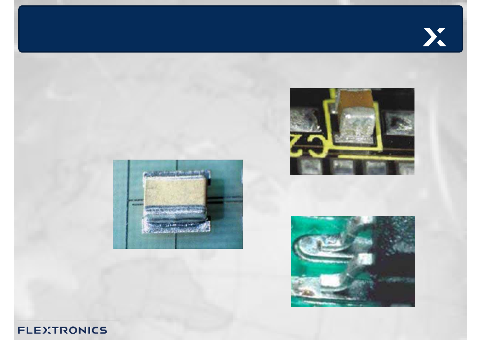
31
No Solder
No Solder
/
/ 无锡
Countermeasure/ 对策
1. Missing printing/ 漏印
Root cause: a) Stencil aperture was jammed./ 钢网堵孔
b) High viscosity of solder paste./ 锡膏粘性过高
Action: a) Clean stencil;/ 清洗钢网
b) Replace the recycled paste with fresh one./更换新锡膏
c) Printing machine parameter adjustment./校正丝印机参数
2. Poor solderability of component or pad./元件或焊盘可焊性太低
Root cause: a) Old date component or PCB. /陈旧元件或PCB板
b) Contamination on component or PCB. /元件或焊盘受污染
Action: Purge the material for further disposition. /清除来料
3. Insufficient flux volume: increase flux spray rate (wave solder).
助焊剂量不足: 增加助焊剂喷射量 (波峰焊接)
4. Preheat excess: lower preheat temperature properly (wave solder).
预热过度: 适当降低预热温度 (波峰焊)
5. Chip wave or solder wave height is low : proper height (wave solder).
波峰高度过低: 调整到适当高度 (波峰焊)
32
Insufficient Solder
Insufficient Solder
/
/
少
少锡
Insufficient
Insufficient solder
焊
焊锡不足
33
Insufficient Solder
Insufficient Solder
/
/
少
少锡
Countermeasure /对策
1. Stencil apertu re clogging cause incomplete solder printing):
Automatic or manual clean the stencil.
钢网孔堵塞导致锡膏不完全印刷: 自动或者手工清洗钢网
2. No enough solder paste volume (Paste height under LCL) :
Visual inspection and Cpk control.
锡膏量不足(锡膏高度在LCL以下): 目检和Cpk控制
3. Solder paste print misalignment: Fine tune printing
machine
锡膏印刷偏位:校正丝印机使之最优
4. Poor solderability of component or PCB pad: 元件或PCB焊盘可焊性差
a) Optimize reflow profile.优化回流曲线
b) Exchange the poor solderability component. 更换掉低可焊性元件
5. Excess glue or glue misalignment: Fine tune screen print (wave solder). 点胶
过多或点胶偏位:优化丝印参数
6. Less flux : Increase the flux spray on board before it pass wave soldering
(wave solder).助焊剂不足: 增加助焊剂的喷射量