SIPLACE HS50 电路图.pdf - 第96页
2 Circuit Diagr ams 96 I 0033615 3-030 104LD3 Di stributo r , sector 4 (Sh. 4 o f 4) +24V C E 4 GND 2 3 2 1 4 GND GND 4 5 6 2 3 8 A 6 X8dn key X9dn key 3 4 6 5 GND 1 X4dn X15dn key E D C 4 5 X3dn X3dn E 1 3 4 6 24V 0V 0V…
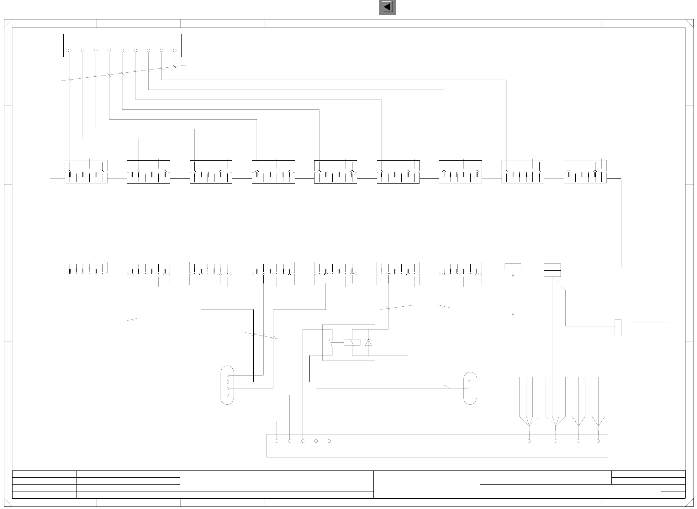
2 Circuit Diagrams 95
I
00336153-030104LD3 Distributor, sector 4 (Sh. 3 of 4)
Bauteilangaben nur zur Information
Weitergabe sowie Vervielfaeltigung dieser Unterlage, Ver-
wertung und Mitteilung ihres Inhalts nicht gestattet, soweit
nicht ausdruecklich zugestanden. Alle Rechte vorbehalten, ins-
besondere fuer den Fall der Patenterteilung oder GM-Eintragung.
Comunicado como segredo empresarial. Reservados todos os direitos.
Confie a titre de secret d’entreprise. Tous droits reserves.
Proprietary data , company confidential . All rights reserved.
Confiado como secrete industrial. Nos reservamos todos los derechos.
Status Modified
Product stat.
Document stat.
Function stat.
Date Name
Author
Stand.
Check.
Date
Orig. Repl. f. Replaced by
SMD Placement System SIPLACE HS50
bk
S_Ready
Ctrl_On
S_Emerg.StopButton
S_hood
S_CompTable
S_KeySwitch
S_StartButton
S_StopButton
S_CompFlap
CAN input/output conveyor 1
Spare
bk
bk
CAN bus
To X17an
(CAN I/O module 2
sheet 4)
S_PressureSensor
Compressed air
Pressure sensor
Pneumatic system
bk
Main fault indicator
Fault indicator 1
Green indicator
Fault indicator 2
Sheet
Sh.
Distributor, sector 4
0.56mm²
0.56mm²
0.56mm²
0.56mm²
=
SIEMENS AG
+
M_SteuerungEin
K1
RS30/24VDC
11
12 A1
0V
X5dm
X1dm
A
24V
24V
0V
GND
X400
5
00336801
X17dn
+24V GND +5V
4
5
2
3
4
6
2
A2
A
4
5
3
4
1
5
0V
0V
key
0V
0V
X1dm
125kbps
E
A
24V
E
X3dm
X14df
1
2
3
4
key
0V
0V
00329698 (dm)
X5dm
GND
E
A
24V
24V
9
0V
X15dm
0V
X12dm
key
X15dm
0V
key
key
X14dm
E
A
A2
X15df
1
2
3
X16dm
2
3
4
1
3
X6dm
2
3
4
5
6
E
24V
24V
X4dm X4dm
A
E
A
24V
24V
0V
0V key
X3dm
24V
24V
GND
3
4
6
1
3
4
X7dm
10
14
12
13
E
A
24V
24V
0V
0V
24V
24V
0V
0V
key
3
X16dm
24V
24V
0V
0V
X14dm
key
24V
key
0V
key
0V
E
7
X6dm
24V
24V
E
A
24V
A
24V
24V
0V
0V
E
0V key
X9dm X9dm
E
A
6
2
3
4
5
1
24V
0V
0V
key
E
X7dm
E
5
B
F
43
3
X8dm X8dm
24V
0V
E
0V
7
8
key
X12dm
E
A
0V
0V
key
X13dm
E
A
A
8
2
3
4
6
2
3
4
24V
24V
A
E
X11dm X11dm
3
4
24V
A
X2dm X2dm
A
1
D
C
3
4
6
2
3
4
5
2
2
A
24V
24V
0V
0V
24V
X13dm
1 4
678
B
5
2
6
F
5
1
11
4
5
1
key
X10dm
X18dm
X17dm
X17dm
X400
24V
D
C
23
5
2
3
4
5
E
5
6
25.03.99
3
00336153-030104LD3
Hoffmann
11.12.1997
27.01.00
25.03.99
04.
01.
03.
Tek
Tek
Tek
4
5
2
3
4
5
6
1
2
3
4
3
4
5
6
1
2
3
4
1
1
4
3
4
6
5
4b
7a
4
5
6
1
2
1
2
3
4
5
6
1
2
24c
1
11a
4c
2
3
PL EA1 E2
1
2
22c
21c
15c
14c
13c
18c
16c
17c
4
5
6
1
2
3
1
2
1
1
1
5
1
2
3
3
4
5
6
1
2
3
1
6
6
6
6
6
6
5
5
2
6
1
2
3
4
5
5
6
5
6
6
19c
3b
6
1
5
6
1
2
3
4
5
2
6
2
5
2
6
1
23c
2b
11b
2
3
4
5
6
1
4
5
3
4
6
6
1
1
2
1
2
3
4
5
6
1
2 Circuit Diagrams 96
I
00336153-030104LD3 Distributor, sector 4 (Sh. 4 of 4)
+24V
C
E
4
GND
2
32
1 4
GND
GND
4
5
6
2
3
8
A
6
X8dn
key
X9dn
key
3
4
6
5
GND
1
X4dn
X15dn
key
E
D
C
4
5
X3dn X3dn
E
1
3
4
6
24V
0V
0V
X2dn X2dn
key
+24V
+24V
E
A
24V
24V
0V
4
5
2
E
A
24V
24V
0V
4
6
1
3
4
00329698 (dn)
A
X17dnX18dn
X10dn
GND
E
E
A
24V
24V
2
3
X16dn
key
2
X17dn
GND
X10df_8
X10df_9
X14dn
24V
A
24V
24V
A
24V
24V
0V
0V
E
A
A
E
X5dn
0V
X10dn
X4dn
E
A
X7dn
E
0V
key
X6dn
key
X7dn
0V
0V
0V
X15dn
E
A
24V
0V
0V
0V
key
4
5
3
4
5
0V
X1dn X1dn
24V
24V
Null
+24V
0V
0V key
125kbps
24V
0V
0V
key
X5dn
4
5
24V
X12dn
E
A
24V
A
24V
X8dn
E
A
0V
0V
X6dn
0V
X13dn
0V
E
A
24V
24V
X11dn
E
A
24V
24V
24V
0V
6
2
3
4
6
24V
0V
0V
A3
3
1
3
4
6
X11dn
2
3
4
6
M_Crash1/4
key
X12dn
key
X13dn
key
M_Crash2/3
2
X400
24V
2
4
5
6
2
key
X9dn
E
1
3
4
0V
key
24V
A
24V
24V
24V
24V
0V
0V
0V
0V
0V
24V
E
X16dn
6
25.03.99
4
00336153-030104LD3
Hoffmann
11.12.1997
27.01.00
25.03.99
04.
01.
03.
Tek
Tek
Tek
4
10:3127.1.2000 /platte_4GB/users/projecte/00336153-03/00336153-030103LD3/schematic/sheet4
2
3
4
5
6
1
2
3
4
5
3
4
5
6
4a
12a
3
4
5
6
1
5
3
4
5
6
1
2
3
4
1
2
6
1
2
2
1
5
3
1
5
2
X18df
1
2
3
4
5
6
1
2
3
4
5
1
2
3
4
5
6
2
3
4
5
6
2
1
2
5
1
X16df
3
4
5
6
1
2
X17df
1
4
3
4
5
6
1
2
3
4
1
2
5
1
1
3
4
5
6
1
2
3
1
2
3
4
5
6
6
5
6
2
6
5
5
6
1
2
3
4
1
6
5
6
1
2
3
4
5
6
5
1
1
3
1
2
3
4
5
6
X19df
1
2
PL EA1 E2
X20df
4
5
6
1
2
1
3
3
4
5
6
3
1
1
5
5
2
5
6
1
2
3
=
SIEMENS AG
+
GND
GND
GND
+24V
A
B
567
876
F
B
F
6
X14dn
key
23
6
2
3
4
6
1
D
Bauteilangaben nur zur Information
Weitergabe sowie Vervielfaeltigung dieser Unterlage, Ver-
wertung und Mitteilung ihres Inhalts nicht gestattet, soweit
nicht ausdruecklich zugestanden. Alle Rechte vorbehalten, ins-
besondere fuer den Fall der Patenterteilung oder GM-Eintragung.
Comunicado como segredo empresarial. Reservados todos os direitos.
Confie a titre de secret d’entreprise. Tous droits reserves.
Proprietary data , company confidential . All rights reserved.
Confiado como secrete industrial. Nos reservamos todos los derechos.
Status Modified
Product stat.
Document stat.
Function stat.
Date Name
Author
Stand.
Check.
Date
Orig. Repl. f. Replaced by
SMD Placement System SIPLACE HS50
Sheet
Sh.
bk
Ctrl_ComponentCounter
Crash / fan unit
S_FanServoOff
Spare
1.0mm²/bk
0.56 mm²/bk
CAN input/output conveyor 2
0.56 mm² / bk
S_LeftNozzles(open)
S_RightNozzles(closed)
Ctrl_ValveNozzles
Nozzle changer 1a
To X17am
(CAN I/O module 1
sheet 3)
CAN bus
Distributor, sector 4
S_LeftNozzles(open)
S_RightNozzles(closed)
Ctrl_ValveNozzles
Nozzle changer 2a
0.56 mm² / bk
Nozzle changer 3a
S_LeftNozzles(open)
S_RightNozzles(closed)
Ctrl_ValveNozzles
0.56 mm² / bk
0.56mm²
0.56 mm² / bk
Nozzle changer 4a
Ctrl_ValveNozzles
S_RightNozzles(closed)
S_LeftNozzles(open)
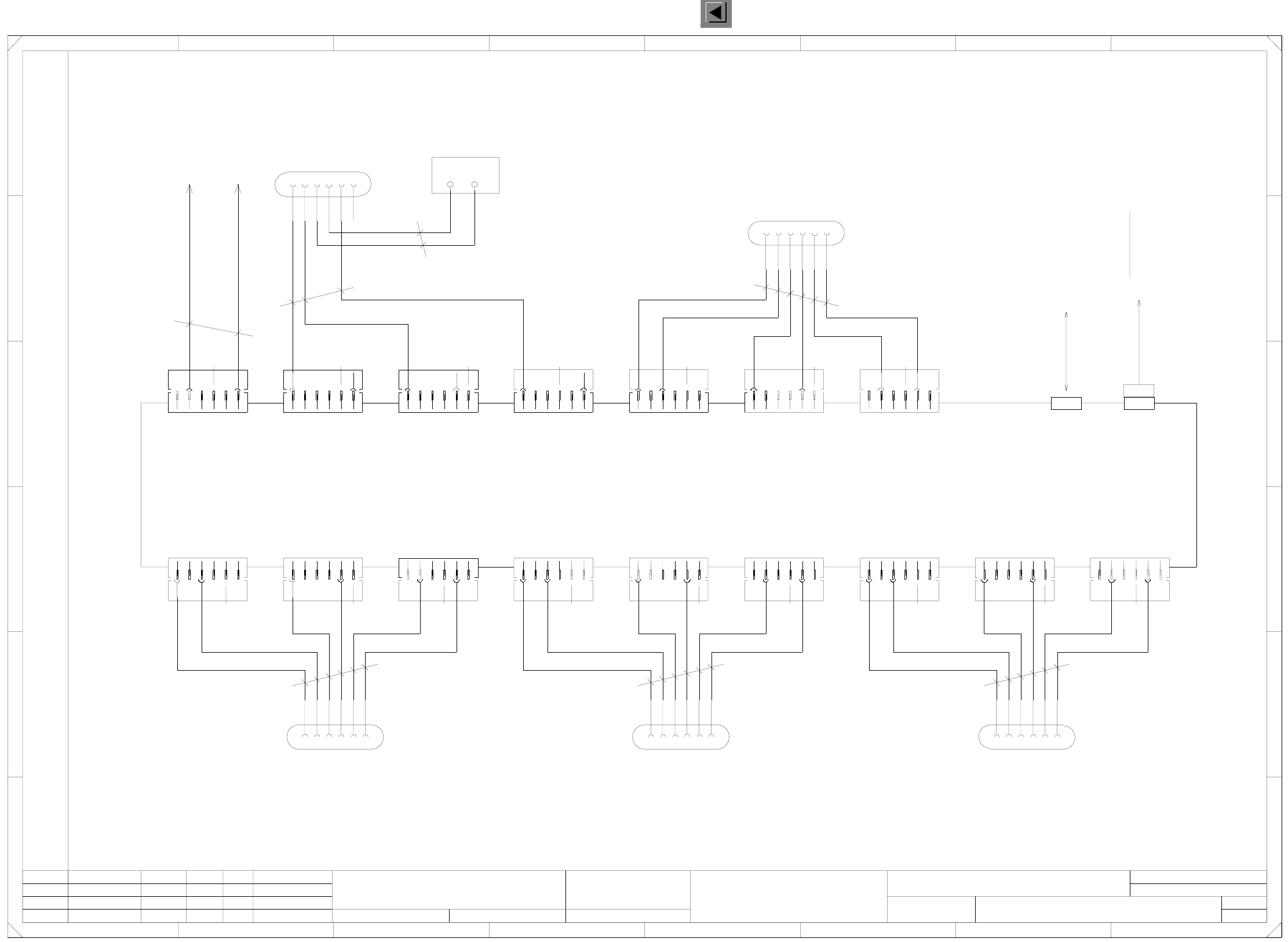
2 Circuit Diagrams 97
I
00336153-030103TD3 Distributor, sector 4
FSUAUSESFS
Weitergabe sowie Vervielfältigung dieser Unterlage, Verwer-
tung und Mitteilung ihres Inhalts nicht gestattet, soweit nicht
ausdrücklich zugestanden. Zuwiderhandlungen verpflichten zu
Schadenersatz. Alle Rechte für den Fall der Patenterteilung
oder GM-Eintragung vorbehalten.
Copying of this document, and giving it to others and the use
or communication of the contents thereof, are forbidden with-
out express authority. Offenders are liable to the payment of
damages. All rights are reserved in the event of the grant of
a patent or the registration of a utility model or design.
SMD Placement System SIPLACE HS50
Distributor, sector 4
Identification: testing engineer, month, year
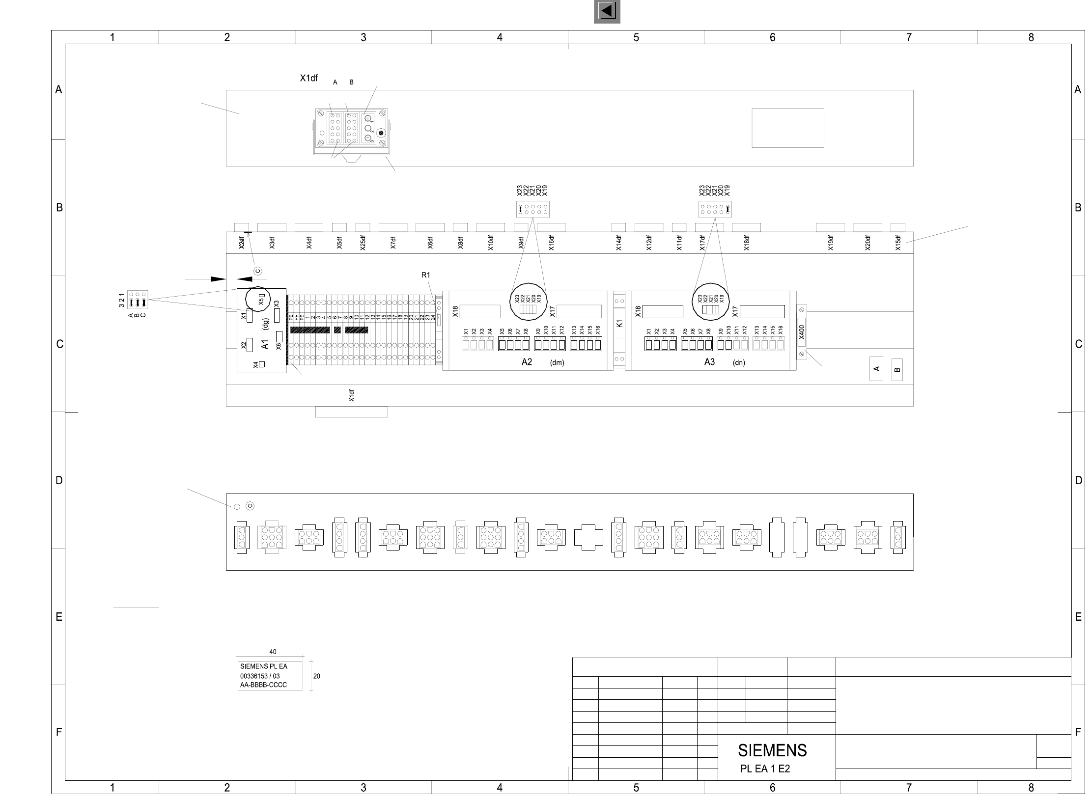
Fon size 2.5 mm, material Scotchal 3698-E (color A1 RAL 9006)
Assembly inscription according to recommendation VA-F-510-001
B: inspection label
A: identification label
The following labels have to be applied:
* Please note
C: PE label (gn/ye)
CCCC = manufacturer/location of plant acc. to SN 37040
BBBB = date (year/month/day) according to SN 01007
AA = numerals
Function status
Document status
Product status
The "PE terminal block" and the ( 1 2 3 ... ) terminal blocks will be connected with an additional yellow/green jumper.
’PE terminal block’ made of a yellow/green 3-pole terminal block
and 2 grey 3-pole terminal blocks with 2 yellow/green jumpers.
Ground hole
Part 001
gn/ye
Pin12
Bracket
Module
Pin1 Pin1
Plug inscription on edge,
font size: 4 mm
Sheet
Sh.
Status Modified Date Name
Author
Check.
Stand.
(Drawing number)
Main no.
Date Name
CAN bus coupler for comp. table 4
Jumper configuration
SLIO module 1, jumper configuration SLIO module 2, jumper configuration
4
Tek
10.04.00
21.04.99
21.04.99
Hoffmann14.01.1998
03.
1
A3
1
00336153-030103TD3
10.04.00
X11df
Part 002
X8dfX4df X6dfX7dfX25dfX5dfX3dfX2df X18dfX17df X20dfX19df X15dfX14dfX16dfX9dfX10df X12df
(Pins 1 and 3 are wired)
Pneumatic module
03.
01.
Tek
Tek