CM602规格说明书(英文).pdf - 第41页
CM602-L 2006.0515 - 36 - 6. PCB Design Standard 6.1 PCB Specifi cations Standard: PCB f ixing m ethod (PC B m arks ar e required.) * For the du al co nve yor, please see “ 4.5 Dual Conve yor (Option) ”. ■ PCB cutout cond…
CM602-L 2006.0515
- 35 -
5. Other Standard Functions
5.1 Programming Functions
All data are created on PT200-G, the data creating device. Some data, however, can be modified on the machine.
The data modified on the machine and what was taught are fed back to PT200-G automatically. Any of the four
corners of PCB can accept the origin of coordinate data.
PS200-G will make data creation more efficient; for example, it distributes data taking the multi-job production
system into consideration.
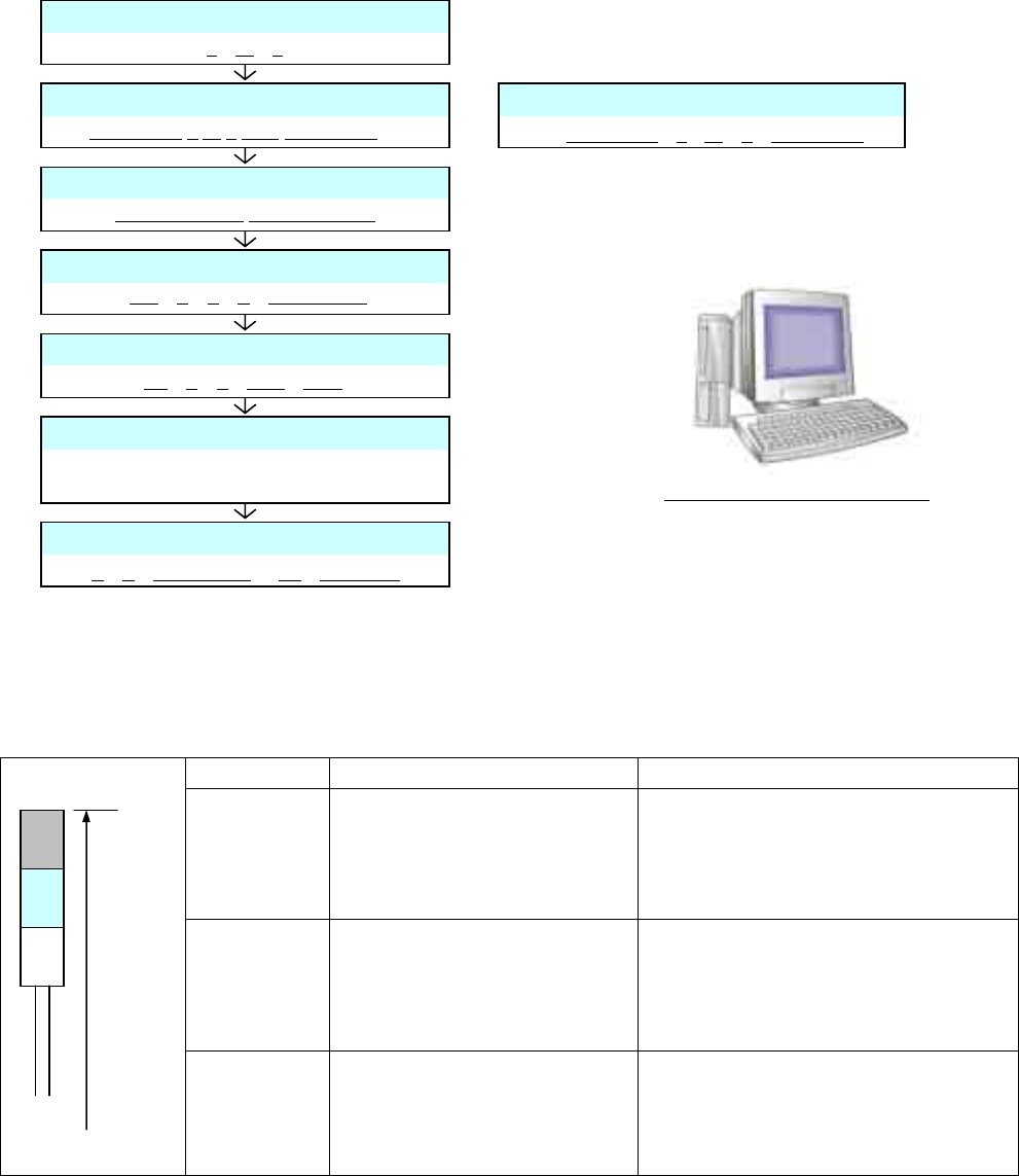
* As for the hardware for PT200-G, prepare by yourself.
Refer to the separate volume, “PT200-G Specification” for details of PT200-G.
Refer to the separate volume, “PS200-G Specification” for details of PS200-G.
5.2 3-Color Signal Tower
Color of signal tower and lighting standard
Signal Color Classification Lighting Standard
Red Emergency stop error
・
Trouble in shafts of motors
・
Drop in air pressure
・
Trouble in PCB supports
・
Head trouble
・
Tape trouble
Yellow Single stop error
・
Pickup error
・
Placement error
・
PCB transfer error
・
No works
・
Nozzle change error
Green
In operation
Electric source ON
(e.g., in automatic operation)
(This, however, is off while red or yel-
low is blinking.)
* Lighting specifications are programmable.
Data creating software PT200-G
PC board Data
L
W
T
Parts Data
Chip Name
L W T REF Style Angle …
Tray Data
Tray Name
L
W
T
Chip Count
Fixation Information
Feeder Fixation
Nozzle Fixation
Max. 10 000
p
oints
Block Data
No.
X
Y
A
Parts Name
Block Attribute Data
BL
X
Y
BAD
ROT
Feeder Arrangement
Nozzle Arrangement
Max. 10 000 points
Placement Data
X
Y
Parts Name
BL Comment
2 000 mm
from floor
(Standard)
Green
Yellow
Red
CM602-L 2006.0515
- 36 -
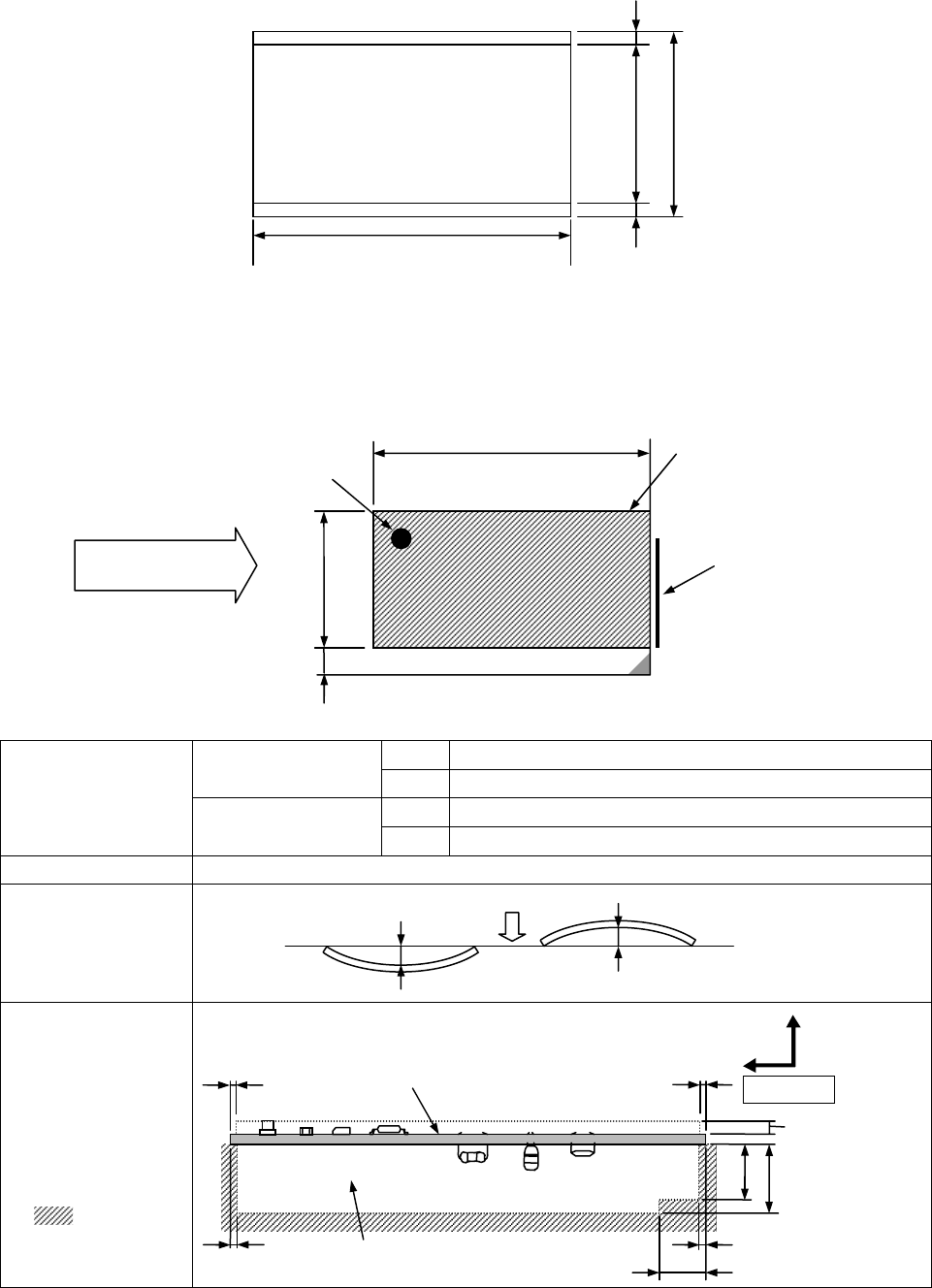
6. PCB Design Standard
6.1 PCB Specifications
Standard: PCB fixing method (PCB marks are required.)
* For the dual conveyor, please see “4.5 Dual Conveyor (Option)”.
■
PCB cutout conditions
To secure the PCB stop position by the PCB stopper and to secure the stable operation of the PCB detection
sensor, the following conditions are set on the position and the dimensions of the PCB cutout.
[The below figure indicates the case of the left to right flow/front reference (standard). Also the other condi-
tions (options) follow this.]
Min. 50 mm × 50 mm
Dimensions
Max. 510 mm × 460 mm
Min. 50 mm × 44 mm
Dimensions
(Placement PCB
Dimensions)
Placement Area
Max. 510 mm × 454 mm
Thickness of PCB 0.3 mm to 4.0 mm
Permissible
PCB warpage
Conditions of PCB
before placement
※
The area
where no components
shall exist.
* For the dual conveyor, please see “4.5 Dual Conveyor (Option)”.
Placement direction
Max. 0.5 mm
Max. 0.5 mm
Open space for transport
3 mm3 mm
3 mm
3 mm
30 mm
25 mm
High Speed head
: Max. 6.5 mm
Multi-functional head
: Max. 21 mm
PCB
20 mm
Y
Z
Fixed side
50 mm to 510 mm
Placement Area
44 mm to 454 mm
50 mm to 460 mm
3 mm3 mm
50 mm
20 mm
4.5 mm
PCB detection sensor position
PCB cutout
prohibited area
PCB flow direction
PCB stopper
CM602-L 2006.0515
- 37 -
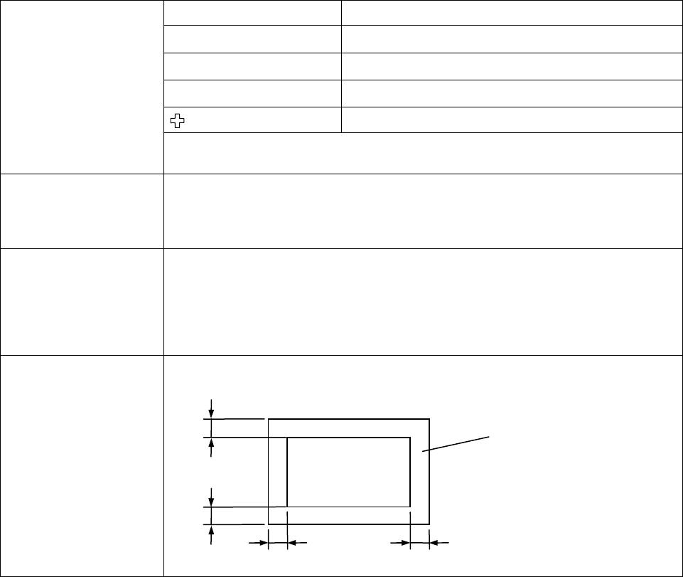
6.2 Recognition Mark
PCB needs two PCB recognition marks at its opposite corners.
■
PCB Recognition Mark Specifications
Standard Mark Shapes Dimensions
○
φ
0.5 mm to
φ
1.6 mm
△
(Equilateral triangle)
Length of one side: 0.5 mm to 1.6 mm
□
Length and width: 0.5 mm to 1.6 mm
Length and width: 0.5 mm to 1.6 mm
Standard Mark Shapes
and Dimensions
Length and width means the dimensions of the quadrangle circumscribing the
mark.
Mark Materials and
Circuit Pattern
Because PCB recognition correction is based on the positional relationship be-
tween the marks and the circuit pattern (conductor pattern), the marks must be
made in the same process and of the same materials as the circuit pattern from
the viewpoint of correction accuracy.
Image Conditions of
Mark Materials and
PCB Base
Because, basically, mark recognition process is carried out based on the inten-
sity difference of reflected light, a fixed contrast is required between the mark
materials and the PCB base.
This difference varies significantly depending on the plating condition, oxidation
condition, surface height, unevenness, degree of mirroring, coating, or distur-
bance light; therefore, the assessment of the marks is required beforehand.
Mark Dimensions and
Background
The background of a mark requires the noninterference area (larger than fixed
dimensions) outside the mark.
Noninterference area
Mark
a
≧
0.2 mm or more
Noninterference area
Not all the marks are black.
a
a
aa