KD-2077_SPE_EN.pdf - 第16页
12 4.5.5 Rec ognitio n mark s hapes The recogn ition marks shall c onform to EIAJ ET - 7302 "Recog nition Marks for Sur face Mounting PW B ." 4.5.5.1 Sha pes • The standar d marks sha ll be 13 ty pes shown in &…
11
4.5 PWB Positioning
4.5.1 PWB positioning reference
Standard: Shape reference
Option: Pin reference
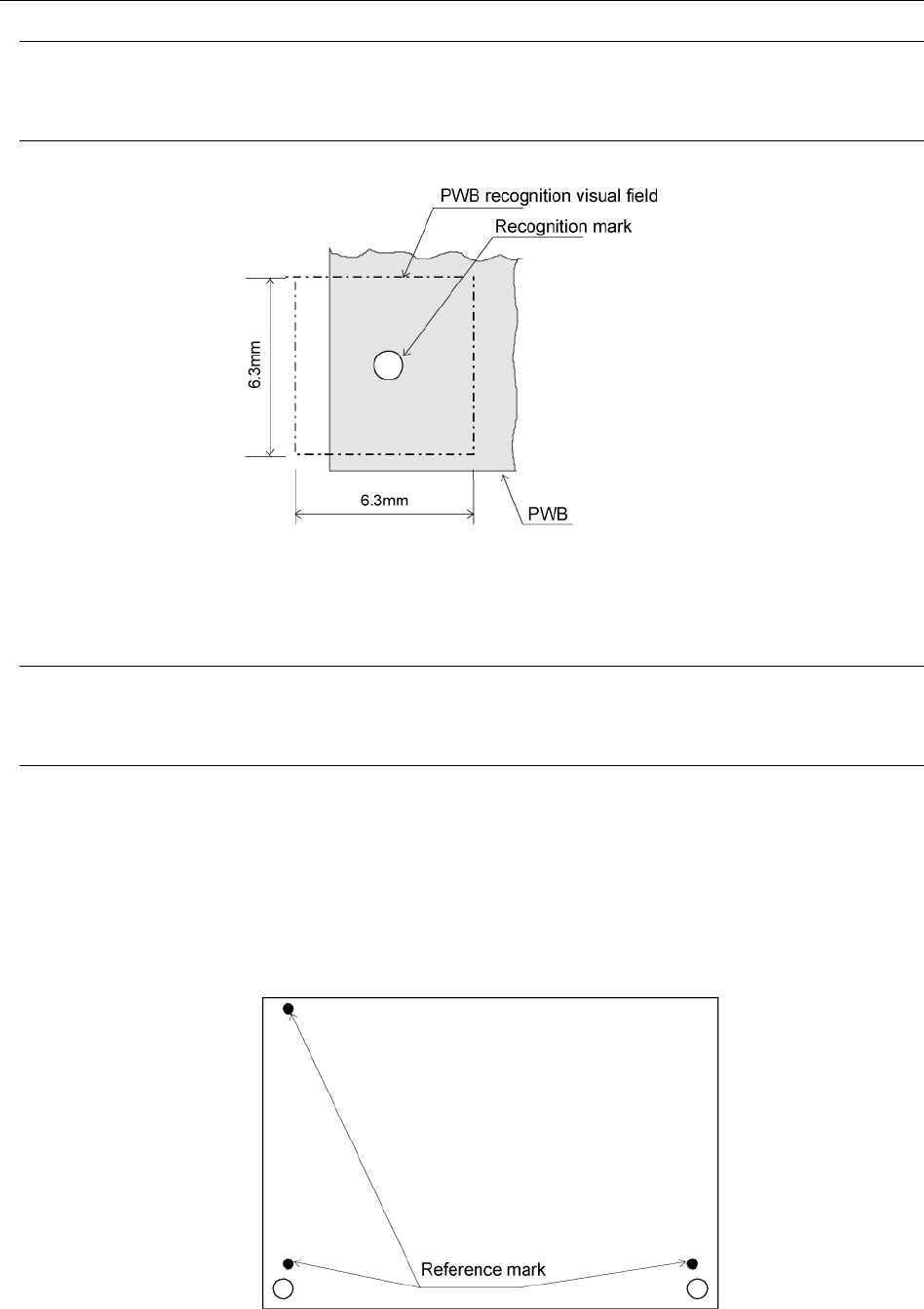
4.5.2 PWB recognition visual field
6.3 mm (camera visual field range)
Figure 5 PWB recognition visual field
4.5.3 Window size
The window size is variable up to 6.3 mm. However, secure a clearance around the recognition
mark.
4.5.4 Recognition mark correction method
The reference marks provided at 2 or 3 positions (Note) are used for positional correction of the
whole PWB. When the marks at 2 positions are detected, the position offset, angle offset, and
PWB expansion/contraction of the whole PWB are corrected. When the 3 marks at 3 positions are
detected, the PWB XY angle offset is additionally corrected.
Note: The positions are optional. Regarding the reference marks at 3 positions, however, these 3
marks must not be aligned on a single straight line. (It is recommended that marks are arranged
at the 4 corners of PWB.)
Figure 6 Reference marks
12
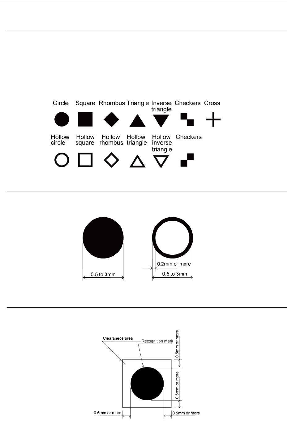
4.5.5 Recognition mark shapes
The recognition marks shall conform to EIAJ ET-7302 "Recognition Marks for Surface Mounting
PWB."
4.5.5.1 Shapes
• The standard marks shall be 13 types shown in "Figure 7 Recognition Mark Shapes."
• Marks other than "Figure 7 Recognition Mark Shapes", the user prepares templates and they
can be recognized by pattern matching.
Note 1: There shall be no patterns of similar shapes except the target mark shapes in the
visual field. Enough contrast shall be obtained.
• Regarding the triangles, checkers, and user's templates, their shapes rotated in a 90-degree
arc can also be recognized.
Figure 7 Recognition mark shapes
4.5.5.2 Size and tolerance
The external size shall be 0 5 mm to 3.0 mm and the tolerance shall be ±10% or less.
For hollow shapes, the line width of the fringe shall be 0.2 mm or more.
Figure 8 Size and tolerance of each recognition mark
4.5.5.3 Clearance
In the periphery of each recognition mark, secure at least 0.5 mm of space in which no
conductor pattern, solder resist or marking exists, from the outer periphery of the recognition
mark.
Figure 9 Clearance for recognition mark
13
4.5.5.4 Basic material
• The basic material shall be non-coated copper or coated copper. (For coating, refer to “4.5.6.5
Coating.”)
• Clear contrast is required between the surface of the recognition mark and the adjacent
printed wire material.
• No oxidation or material deterioration shall be found on the recognition mark.
4.5.5.5 Coating
The surface of the recognition mark shall undergo the following coating.
• Transparent anti-oxidant coating
• Nickel plating
• Tin plating
• Gold plating
• Hot air leveler solder coating
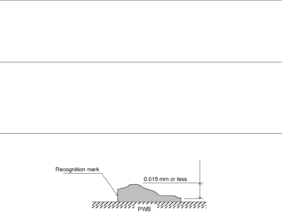
4.5.5.6 Flatness
The difference of altitude on each recognition mark surface shall be 0.015 mm or less.
Regarding flux, coating unevenness shall be found.
Figure 10 Cross section and difference of altitude of the recognition mark