S25 circuit.pdf - 第107页
5 Printed circuit boar ds 107 0032121 3-040 101ND 4 Adjus tment u nit, SP 6_12 pl acem ent head A 12 34 SMD Placement System SIPLACE HS50 00321213-040101ND4 5 Adjustment unit 67 8 1 + = Sheet Sh. 1 F E D 56 7 C B 8 A SP6…
5 Printed circuit boards 106
00308443-050101ND4 Discharge board
00320854-020202MD4 745 PCB, backplane - servo Y1002
Function status
Product status
Doc. status
02
02
02
Zust. Mitteilung Datum
15.04.96
15.04.96 DO
DO
Name
SIEMENS AG
FSZ MUENCHEN
MS-Dorn
03.07.95Datum
Name
00320854-020202MD4
backplane - servo Y1002
745 printed circuit board
SIPLACE
M 1:1
Shee
t
1-
Component diagram, bottom
ANL A441 TD FSZ E
DO15.04.96
Component diagram, top
Wire infeed
Apply the following labels:
A: Identification label
Max. component height:
B: Inspection label
Top = 19mm
Bottom = 34 mm
Remove pins marked 'x'
1.
5.
1.
28.05.96
28.05.96
28.05.96 Tu.
Tu.
Tu.
28.05.1996
28.05.1996
00308443-050101ND4
SIEMENS
Aktiengesellschaft
AUT 5 BPB BS1
Datum
Bearb.
Gepr.
Norm
Name
Dateiname:
Zust.
Mitteilung
Datum
Name
(Materialnummer)
Format A4
Mat.-Nr.: FS ES US S/F
Blatt
Maßstab
Weitergabe sowie Vervielfältigung dieser Unterlage, Verwertung und Mitteilung
ihres Inhaltes nicht gestattet, soweit nicht ausdrücklich zugestanden.
Zuwiderhandlungen verpflichten zu Schadenersatz. Alle Rechte für den Fall
der Patenterteilung oder GM-Eintragung vorbehalten.
Copying of this document, and giving it to others and the use or communication
of the contents thereof, are forbidden without express authority. Offenders are
liable to the payment of damages. All rights are reserved in the event of the
grant of a patent or the registration of the utility model or design.
(a1_1zu1.vsd)
00308443.51N
75 mm
72 mm
1/1
R1
K1
R2 R3
K2 K3
V3 V8
V4
V5
V7
V6
V11
V10
V9
V2
R4
R5
A
B
X1
X2
V1
1
Zeichn.Nr.alt:
1710470-Y0034-000-04
Siemens AUT5
00308443-05
AA-BBBB-CCCC
15
10
Function status
Document status
Product status
SMD Placement System Siplace
Discharge board
The following labels have to be stuck on:
A: Identification label
B: Inspection label
Assembly inscription acc. to recommendation VA-F-510-001
font size 1.5 mm, mat. Scotchcal 3698-E ( color A1 Ral 9006 )
AA = manufacturer/location acc. to SN 37040
BBBB = date (year/month/day) acc. to SN 01007
CCCC = numeral
Product inspection certification acc. to recommendation VA Q 509-001
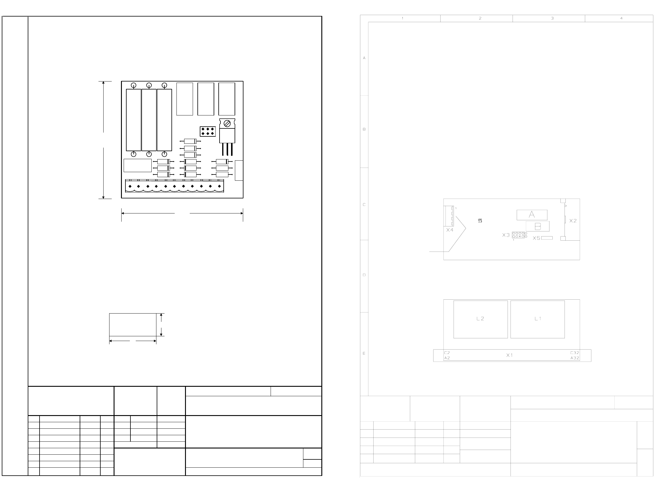
5 Printed circuit boards 107
00321213-040101ND4 Adjustment unit, SP6_12 placement head
A
1234
SMD Placement System SIPLACE HS50
00321213-040101ND4
5
Adjustment unit
678
1
+
=
Sheet
Sh.
1
F
E
D
567
C
B
8
A
SP6_12 placement head
R2
R2R2
R2 R2
V2
V1
X2
X3
h1
h2
SIEMENS AG
Bearb.
Norm
Datum
1.
1.
4.
Zustand
F
Aenderung
1
NameDatum
Doc. status
Product status
Function status
Gepr.
E
D
Urspr.
23
19.06.97
PL EA1 E2
Ers. f.
4
Ers. d.
C
B
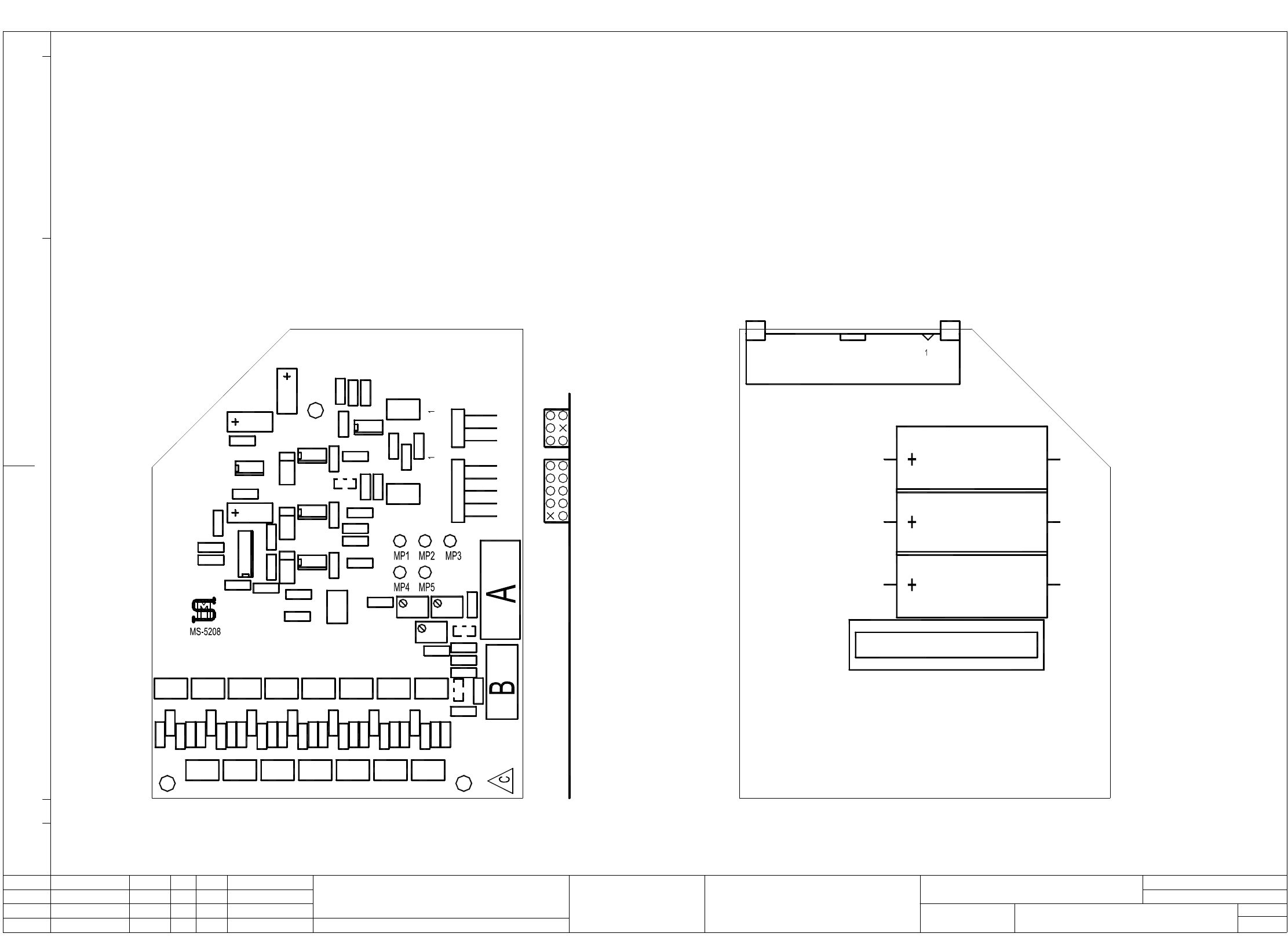
5 Printed circuit boards 108
00321469-040101ND3 CO illumination
X4 X1
Remove all pins marked with an x.
The following labels have to be stuck on!
C1 to C3 have to be glued!
A: Identification label
B: Inspection label
C: ESD label
R14
V4V5
R35
R26
R36
R9
R17
Siemens AG
AUT5-BSM
MS-Elektronik
Zustand
01.
04.
25.11.98
Datum
Document. status
Aenderung Name
Hi
Norm
Gepr.
25.11.98
Function status
1
Dorn
2
Datum
Beab.
6
Urspr./Ers.f./Ers.d.
25.11.98
345 789
00321469-040101ND3
Components illumination
Stromlaufplan/Circuit diagram
10 11 12
SIPLACE HS50
13 14 15
Sh.
V14 V13V17 V16 V15
V6
R27
V7V8
R12
R38
R29
R11
R20
1716 18
Sh.1
1
19
R52
V3
V12
R15
Maximum component height: ON TOP 10.0 mm, ON BOTTOM 14.0 mm
R56
V11
V18
V9
R39
V10
R13
R31
R21
R30
R53
V19
R2
R57
R1
R58
R5
V2
R4
R22
C8
J2
J1
J3
V23
R54
C10
R45
R44
J4
V24
R41
R40
R32
R23
C12
C11
J5
C5
C4
C6
C7
R50
J6
C13
C9
R37
R28
R10
R19
R18
X3
X2
C2
C3
C1
V22
R48
R3
R47
R42
R34
R25
R8
R7
R16
P1
V1
R55
V21
R43
R33
R24
R6
R49
R46
R51
V20
P2
P3
Product status
01.
25.11.98