Samsung(三星)-KLM8G1GEAC-B001.pdf - 第21页
- 20 - IF THERE IS ANY OTHER OPERATION TO IMPLEMENT IN ADDITION TO SPECIFICATION IN THE DATASHEET OR JEDEC STANDARD, PLEASE CONTACT EACH BRANCH OFFICE OR HEADQUARTERS OF SAMSUNG ELECTRONICS. datasheet e·MMC Rev. 1.0 KLMx…
- 19 -
IF THERE IS ANY OTHER OPERATION TO IMPLEMENT IN ADDITION TO SPECIFICATION
IN THE DATASHEET OR JEDEC STANDARD, PLEASE CONTACT EACH BRANCH OFFICE OR
HEADQUARTERS OF SAMSUNG ELECTRONICS.
datasheet
e·MMC
Rev. 1.0
KLMxGxGEAC-B001
SAMSUNG CONFIDENTIAL
6.0 REGISTER VALUE
6.1 OCR Register
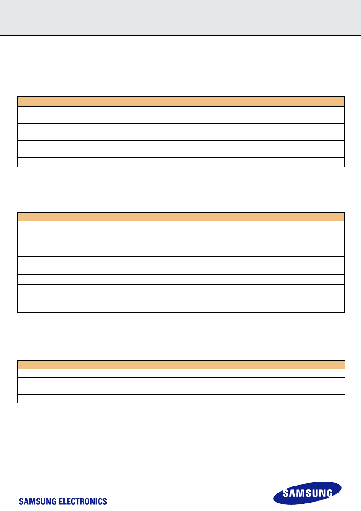
The 32-bit operation conditions register stores the VDD voltage profile of the e·MMC. In addition, this register includes a status information bit. This status
bit is set if the e·MMC power up procedure has been finished. The OCR register shall be implemented by all e·MMCs.
[Table 30] OCR Register
NOTE :
1) This bit is set to LOW if the e·MMC has not finished the power up routine
2) The voltage for internal flash memory(VDDF) should be 2.7-3.6v regardless of OCR Register value.
6.2 CID Register
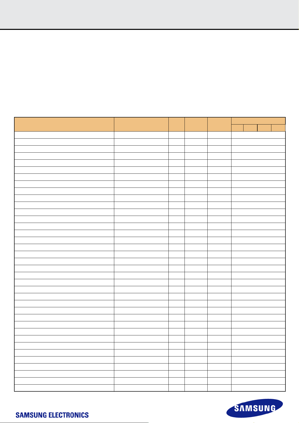
[Table 31] CID Register
NOTE :
1),4),5) description are same as e.MMC JEDEC standard
2) PRV is composed of the revision count of controller and the revision count of F/W patch
3) A 32 bits unsigned binary integer. (Random Number)
6.2.1 Product name table (In CID Register)
[Table 32] Product name table
OCR bit
VDD voltage window
2
Register Value
[6:0] Reserved 00 00000b
[7] 1.70 - 1.95 1b
[14:8] 2.0-2.6 000 0000b
[23:15] 2.7-3.6 1 1111 1111b
[28:24] Reserved 0 0000b
[30:29] Access Mode 00b (byte mode) 10b (sector mode) -[ *Higher than 2GB only]
[31]
e·MMC power up status bit (busy)
1
Name Field Width CID-slice CID Value
Manufacturer ID MID 8 [127:120] 0x15
Reserved 6 [119:114] ---
Card/BGA CBX 2 [113:112] 01
OEM/Application ID OID 8 [111:104]
---
1
Product name PNM 48 [103:56] See Product name table
Product revision PRV 8 [55:48]
---
2
Product serial number PSN 32 [47:16]
---
3
Manufacturing date MDT 8 [15:8]
---
4
CRC7 checksum CRC 7 [7:1]
---
5
not used, always ’1’ - 1 [0:0] ---
Part Number Density Product Name in CID Register (PNM)
KLM8G1GEAC-B001 8 GB 0 x 4D3847314743
KLMAG2GEAC-B001 16 GB 0 x 4D4147324743
KLMBG4GEAC-B001 32 GB 0 x 4D4247344743
KLMCG8GEAC-B001 64 GB 0 x 4D4347384743
- 20 -
IF THERE IS ANY OTHER OPERATION TO IMPLEMENT IN ADDITION TO SPECIFICATION
IN THE DATASHEET OR JEDEC STANDARD, PLEASE CONTACT EACH BRANCH OFFICE OR
HEADQUARTERS OF SAMSUNG ELECTRONICS.
datasheet
e·MMC
Rev. 1.0
KLMxGxGEAC-B001
SAMSUNG CONFIDENTIAL
6.3 CSD Register
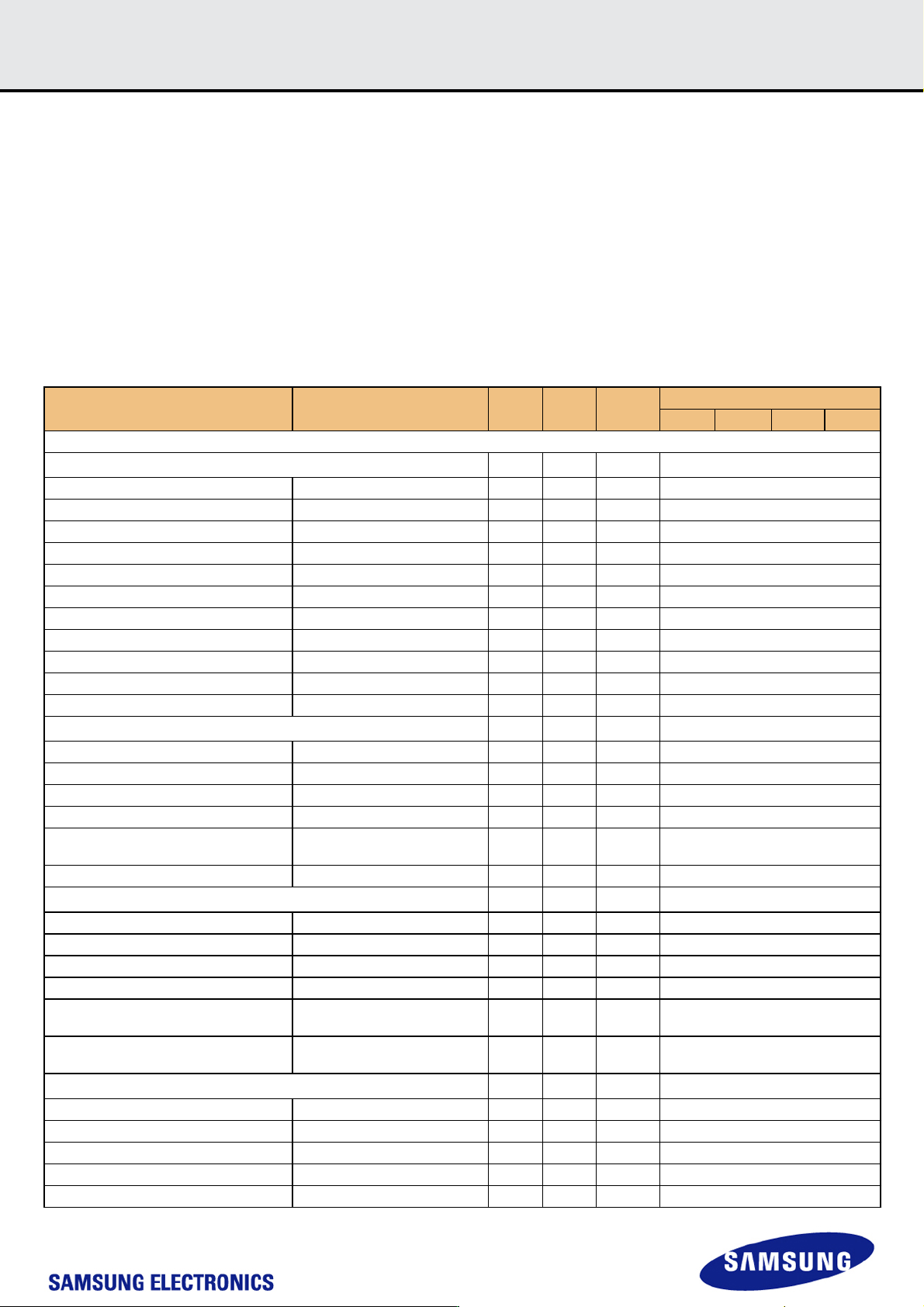
The Card-Specific Data register provides information on how to access the e·MMC contents. The CSD defines the data format, error correction type, max-
imum data access time, data transfer speed, whether the DSR register can be used etc. The programmable part of the register (entries marked by W or
E, see below) can be changed by CMD27. The type of the entries in the table below is coded as follows:
R : Read only
W: One time programmable and not readable.
R/W: One time programmable and readable.
W/E : Multiple writable with value kept after power failure, H/W reset assertion and any CMD0 reset and not readable.
R/W/E: Multiple writable with value kept after power failure, H/W reset assertion and any CMD0 reset and readable.
R/W/C_P: Writable after value cleared by power failure and HW/ rest assertion (the value not cleared by CMD0 reset) and readable.
R/W/E_P: Multiple writable with value reset after power failure, H/W reset assertion and any CMD0 reset and readable.
W/E/_P: Multiple wtitable with value reset after power failure, H/W reset assertion and any CMD0 reset and not readable.
[Table 33] CSD Register
Name Field Width Cell Type CSD-slice
CSD Value
8GB 16GB 32GB 64GB
CSD structure CSD_STRUCTURE 2 R [127:126] 0x03
System specification version SPEC_VERS 4 R [125:122] 0x04
Reserved - 2 R [121:120] -
Data read access-time 1 TAAC 8 R [119:112] 0x27
Data read access-time 2 in CLK cycles (NSAC*100) NSAC 8 R [111:104] 0x01
Max. bus clock frequency TRAN_SPEED 8 R [103:96] 0x32
Device command classes CCC 12 R [95:84] 0xF5
Max. read data block length READ_BL_LEN 4 R [83:80] 0x09
Partial blocks for read allowed READ_BL_PARTIAL 1 R [79:79] 0x00
Write block misalignment WRITE_BLK_MISALIGN 1 R [78:78] 0x00
Read block misalignment READ_BLK_MISALIGN 1 R [77:77] 0x00
DSR implemented DSR_IMP 1 R [76:76] 0x00
Reserved - 2 R [75:74] -
Device size C_SIZE 12 R [73:62] 0xFFF
Max. read current @ VDD min VDD_R_CURR_MIN 3 R [61:59] 0x06
Max. read current @ VDD max VDD_R_CURR_MAX 3 R [58:56] 0x06
Max. write current @ VDD min VDD_W_CURR_MIN 3 R [55:53] 0x06
Max. write current @ VDD max VDD_W_CURR_MAX 3 R [52:50] 0x06
Device size multiplier C_SIZE_MULT 3 R [49:47] 0x07
Erase group size ERASE_GRP_SIZE 5 R [46:42] 0x1F
Erase group size multiplier ERASE_GRP_MULT 5 R [41:37] 0x1F
Write protect group size WP_GRP_SIZE 5 R [36:32] 0x0F
Write protect group enable WP_GRP_ENABLE 1 R [31:31] 0x01
Manufacturer default ECC DEFAULT_ECC 2 R [30:29] 0x00
Write speed factor R2W_FACTOR 3 R [28:26] 0x03
Max. write data block length WRITE_BL_LEN 4 R [25:22] 0x09
Partial blocks for write allowed WRITE_BL_PARTIAL 1 R [21:21] 0x00
Reserved - 4 R [20:17] -
Content protection application CONTENT_PROT_APP 1 R [16:16] 0x00
File format group FILE_FORMAT_GRP 1 R/W [15:15] 0x00
Copy flag (OTP) COPY 1 R/W [14:14] 0x01
Permanent write protection PERM_WRITE_PROTECT 1 R/W [13:13] 0x00
Temporary write protection TMP_WRITE_PROTECT 1 R/W/E [12:12] 0x00
File format FILE_FORMAT 2 R/W [11:10] 0x00
ECC code ECC 2 R/W/E [9:8] 0x00
CRC CRC 7 R/W/E [7:1] -
Not used, always’1’ - 1 — [0:0] -
- 21 -
IF THERE IS ANY OTHER OPERATION TO IMPLEMENT IN ADDITION TO SPECIFICATION
IN THE DATASHEET OR JEDEC STANDARD, PLEASE CONTACT EACH BRANCH OFFICE OR
HEADQUARTERS OF SAMSUNG ELECTRONICS.
datasheet
e·MMC
Rev. 1.0
KLMxGxGEAC-B001
SAMSUNG CONFIDENTIAL
6.4 Extended CSD Register
The Extended CSD register defines the e·MMC properties and selected modes. It is 512 bytes long.
The most significant 320 bytes are the Properties segment, which defines the e·MMC capabilities and cannot be modified by the host. The lower 192
bytes are the Modes segment, which defines the configuration the e·MMC is working in. These modes can be changed by the host by means of the
SWITCH command.
R : Read only
W: One time programmable and not readable.
R/W: One time programmable and readable.
W/E : Multiple writable with value kept after power failure, H/W reset assertion and any CMD0 reset and not readable.
R/W/E: Multiple writable with value kept after power failure, H/W reset assertion and any CMD0 reset and readable.
R/W/C_P: Writable after value cleared by power failure and HW/ rest assertion (the value not cleared by CMD0 reset) and readable.
R/W/E_P: Multiple writable with value reset after power failure, H/W reset assertion and any CMD0 reset and readable.
W/E/_P: Multiple wtitable with value reset after power failure, H/W reset assertion and any CMD0 reset and not readable
[Table 34] Extended CSD Register
Name Field
Size
(Bytes)
Cell
Type
CSD
slice
CSD Value
8GB 16GB 32GB 64GB
Properties Segment
Reserved
1
7 - [511:505] -
Supported Command Sets S_CMD_SET 1 R [504] 0x01
HPI features HPI_FEATURES 1 R [503] 0x01
Background operations support BKOPS_SUPPORT 1 R [502] 0x01
Max packed read commands MAX_PACKED_READS 1 R [501] 0x3F
Max packed write commands MAX_PACKED_WRITES 1 R [500] 0x3F
Data Tag Support DATA_TAG_SUPPORT 1 R [499] 0x01
Tag Unit Size TAG_UNIT_SIZE 1 R [498] 0x04
Tag Resources Size TAG_RES_SIZE 1 R [497] 0x00
Context management capabilities CONTEXT_CAPABILITIES 1 R [496] 0x05
Large Unit size LARGE_UNIT_SIZE_M1 1 R [495] 0x07
Extended partitions attribute support EXT_SUPPORT 1 R [494] 0x03
Reserved
1
241 - [493:253] -
Cache size CACHE_SIZE 4 R [252:249] 0x10000
Generic CMD6 timeout GENERIC_CMD6_TIME 1 R [248] 0x0A
Power off notification(long) timeout POWER_OFF_LONG_TIME 1 R [247] 0x3C
Background operations status BKOPS_STATUS 1 R [246] 0x00
Number of correctly programmed sectors
CORRECTLY_PRG_SECTORS_
NUM
4 R [245:242] 0x00
1st initialization time after partitioning INI_TIMEOUT_AP 1 R [241] 0x1E
Reserved
1
1 - [240] -
Power class for 52MHz, DDR at 3.6V PWR_CL_DDR_52_360 1 R [239] 0x00
Power class for 52MHz, DDR at 1.95V PWR_CL_DDR_52_195 1 R [238] 0x00
Power class for 200MHz at 3.6V PWR_CL_200_360 1 R [237] 0x00
Power class for 200MHz, at 1.95V PWR_CL_200_195 1 R [236] 0x00
Minimum Write Performance for 8bit at
52MHz in DDR mode
MIN_PERF_DDR_W_8_52 1 R [235] 0x00
Minimum Read Performance for 8bit at
52MHz in DDR mode
MIN_PERF_DDR_R_8_52 1 R [234] 0x00
Reserved
1
1 - [233] -
TRIM Multiplier TRIM_MULT 1 R [232] 0x02
Secure Feature support SEC_FEATURE_SUPPORT 1 R [231] 0x55
Secure Erase Multiplier SEC_ERASE_MULT 1 R [230] 0x1B
Secure TRIM Multiplier SEC_TRIM_MULT 1 R [229] 0x11
Boot information BOOT_INFO 1 R [228] 0x07