Samsung(三星)-KLM8G1GEAC-B001.pdf - 第5页
- 4 - IF THERE IS ANY OTHER OPERATION TO IMPLEMENT IN ADDITION TO SPECIFICATION IN THE DATASHEET OR JEDEC STANDARD, PLEASE CONTACT EACH BRANCH OFFICE OR HEADQUARTERS OF SAMSUNG ELECTRONICS. datasheet e·MMC Rev. 1.0 KLMxG…
Table Of Contents
- 4 -
IF THERE IS ANY OTHER OPERATION TO IMPLEMENT IN ADDITION TO SPECIFICATION
IN THE DATASHEET OR JEDEC STANDARD, PLEASE CONTACT EACH BRANCH OFFICE OR
HEADQUARTERS OF SAMSUNG ELECTRONICS.
datasheet
e·MMC
Rev. 1.0
KLMxGxGEAC-B001
SAMSUNG CONFIDENTIAL
1.0 PRODUCT LIST..........................................................................................................................................................4
2.0 KEY FEATURES.........................................................................................................................................................4
3.0 PACKAGE CONFIGURATIONS .................................................................................................................................5
3.1 153 Ball Pin Configuration .......................................................................................................................................5
3.1.1 11.5mm x 13mm x 1.0mm Package Dimension................................................................................................6
3.1.2 11.5mm x 13mm x 1.2mm Package Dimension................................................................................................7
3.2 Product Architecture ................................................................................................................................................8
4.0 e.MMC 4.5 features ....................................................................................................................................................9
4.1 Packed Command ...................................................................................................................................................9
4.2 Cache ......................................................................................................................................................................11
4.3 Discard .................................................................................................................................................................... 12
4.4 Sanitize....................................................................................................................................................................13
4.5 Power Off Notification..............................................................................................................................................14
5.0 Technical Notes ..........................................................................................................................................................15
5.1 S/W Agorithm ..........................................................................................................................................................15
5.1.1 Partition Management .......................................................................................................................................15
5.1.1.1 Boot Area Partition and RPMB Area Partition ............................................................................................15
5.1.1.2 Enhanced Partition (Area) ..........................................................................................................................15
5.1.2 Boot operation...................................................................................................................................................16
5.1.3 User Density......................................................................................................................................................17
5.1.4 Auto Power Saving Mode..................................................................................................................................18
5.1.5 Performance......................................................................................................................................................18
6.0 REGISTER VALUE.....................................................................................................................................................19
6.1 OCR Register ..........................................................................................................................................................19
6.2 CID Register ............................................................................................................................................................19
6.2.1 Product name table (In CID Register) ...............................................................................................................19
6.3 CSD Register...........................................................................................................................................................20
6.4 Extended CSD Register ..........................................................................................................................................21
7.0 AC PARAMETER........................................................................................................................................................25
7.1 Timing Parameter ....................................................................................................................................................25
7.2 Previous Bus Timing Parameters for DDR52 are defined by JEDEC standard.......................................................25
7.3 Bus Timing Specification in HS200 mode ...............................................................................................................26
7.3.1 HS200 Clock Timing .........................................................................................................................................26
7.3.2 HS200 Device Input Timing ..............................................................................................................................26
7.3.3 HS200 Device Output Timing............................................................................................................................27
7.4 Bus signal levels......................................................................................................................................................28
7.4.1 Open-drain mode bus signal level.....................................................................................................................28
7.4.2 Push-pull mode bus signal level eMMC ............................................................................................................28
8.0 DC PARAMETER .......................................................................................................................................................29
8.1 Active Power Consumption during operation ..........................................................................................................29
8.2 Standby Power Consumption in auto power saving mode and standby state........................................................29
8.3 Sleep Power Consumption in Sleep State..............................................................................................................29
8.4 Supply Voltage ........................................................................................................................................................ 29
8.5 Bus Signal Line Load...............................................................................................................................................30
9.0 e·MMC Connection Guide ..........................................................................................................................................31
9.1 x8 support Host connection Guide ..........................................................................................................................31
9.2 x4 support Host connection Guide ..........................................................................................................................31
- 4 -
IF THERE IS ANY OTHER OPERATION TO IMPLEMENT IN ADDITION TO SPECIFICATION
IN THE DATASHEET OR JEDEC STANDARD, PLEASE CONTACT EACH BRANCH OFFICE OR
HEADQUARTERS OF SAMSUNG ELECTRONICS.
datasheet
e·MMC
Rev. 1.0
KLMxGxGEAC-B001
SAMSUNG CONFIDENTIAL
INTRODUCTION
The SAMSUNG e·MMC is an embedded MMC solution designed in a BGA package form. e·MMC operation is identical to a MMC card and therefore is a
simple read and write to memory using MMC protocol v4.5 which is a industry standard.
e·MMC consists of NAND flash and a MMC controller. 3V supply voltage is required for the NAND area (VDDF) whereas 1.8V or 3V dual supply voltage
(VDD) is supported for the MMC controller. Maximum MMC interface frequency of 200MHz and maximum bus widths of 8 bit are supported.
There are several advantages of using e·MMC. It is easy to use as the MMC interface allows easy integration with any microprocessor with MMC host.
Any revision or amendment of NAND is invisible to the host as the embedded MMC controller insulates NAND technology from the host. This leads to
faster product development as well as faster times to market.
The embedded flash mangement software or FTL(Flash Transition Layer) of e·MMC manages Wear Leveling, Bad Block Management and ECC. The
FTL supports all features of the Samsung NAND flash and achieves optimal performance.
1.0 PRODUCT LIST
[Table 1] Product List
2.0 KEY FEATURES
embeddedMultiMediaCard System Specification Ver. 4.5 compatible. Detail description is referenced by JEDEC Standard
SAMSUNG e·MMC supports new e·MMC4.5 features defined by JEDEC Standard
- Supported Features : Packed command, Cache, Discard, Sanitize, Power Off Notification, Data Tag,
Partition types, Context ID, Real Time Clock, Dynamic Device Capacity, HS200
- Non-supported Features : Large Sector Size (4KB)
Full backward compatibility with previous MultiMediaCard system specificataion (1bit data bus, multi-e·MMC systems)
Data bus width : 1bit (Default) , 4bit and 8bit
MMC I/F Clock Frequency : 0 ~ 200MHz
MMC I/F Boot Frequency : 0 ~ 52MHz
Temperature : Operation(-25C ~ 85C), Storage without operation (-40C ~ 85C)
Power : Interface power → VDD (1.70V ~ 1.95V or 2.7V ~ 3.6V) , Memory power → VDDF(2.7V ~ 3.6V)
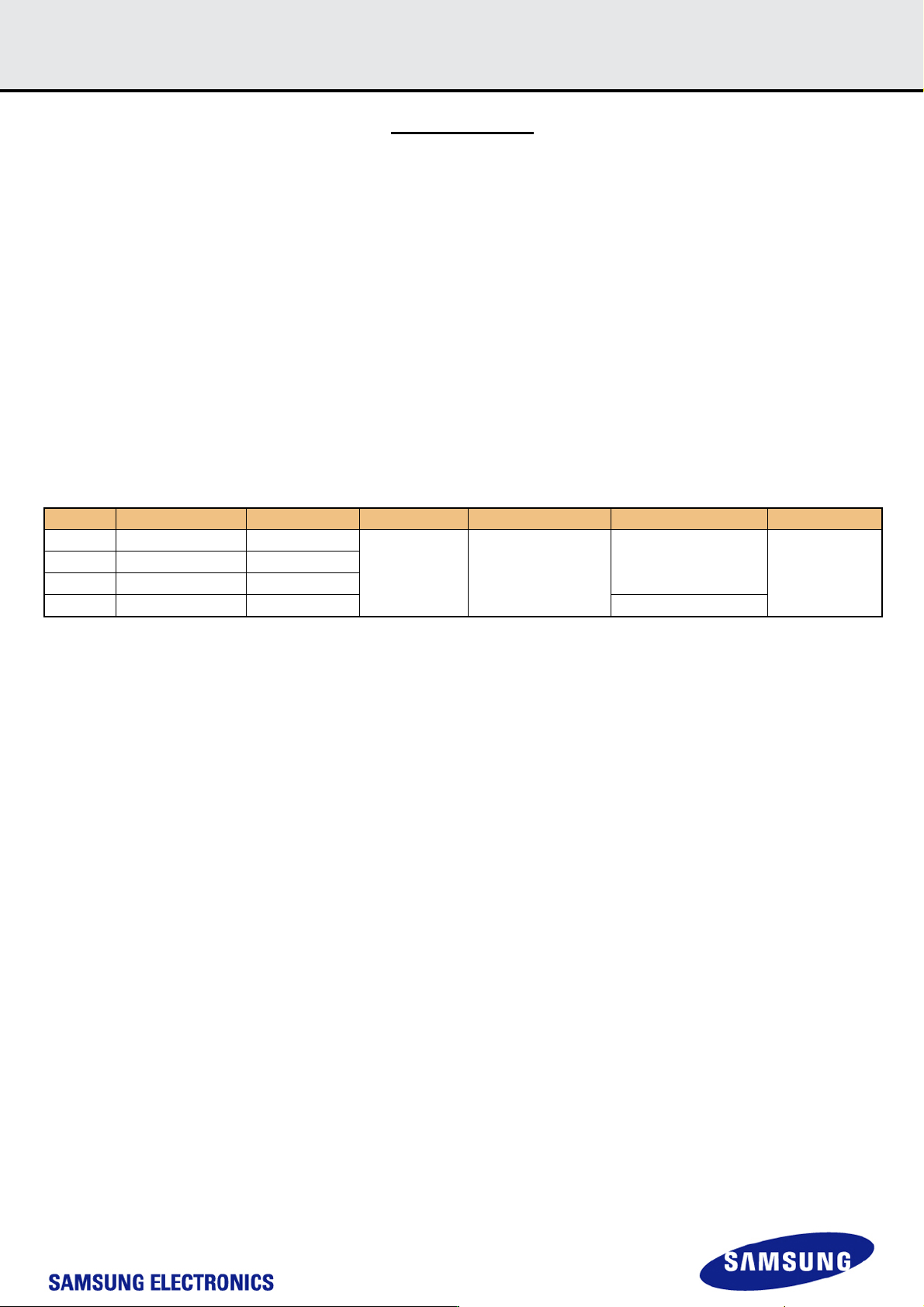
Capacities e·MMC Part ID NAND Flash Type User Density (%) Power System Package size Pin Configuration
8 GB KLM8G1GEAC-B001 64Gb x 1
91.0%
- Interface power : VDD
(1.70V ~ 1.95V or
2.7V ~ 3.6V)
- Memory power :
VDDF (2.7V ~ 3.6V)
11.5mm x 13mm x 1.0mm
153FBGA
16 GB KLMAG2GEAC-B001 64Gb x 2
32 GB KLMBG4GEAC-B001 64Gb x 4
64 GB KLMCG8GEAC-B001 64Gb x 8 11.5mm x 13mm x 1.2mm
- 5 -
IF THERE IS ANY OTHER OPERATION TO IMPLEMENT IN ADDITION TO SPECIFICATION
IN THE DATASHEET OR JEDEC STANDARD, PLEASE CONTACT EACH BRANCH OFFICE OR
HEADQUARTERS OF SAMSUNG ELECTRONICS.
datasheet
e·MMC
Rev. 1.0
KLMxGxGEAC-B001
SAMSUNG CONFIDENTIAL
3.0 PACKAGE CONFIGURATIONS
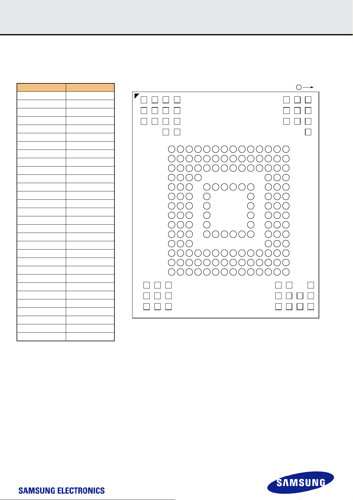
3.1 153 Ball Pin Configuration
[Table 2] 153 Ball Information
Figure 1. 153-FBGA
CLK : Clock input
CMD : A bidirectional signal used for device initialization and command transfers.
Command operates in two modes, open-drain for initialization and push-pull for fast command transfer.
DAT0-7 : Bidirectional data channels. It operates in push-pull mode.
RST_n : H/W reset signal pin
VDDF(VCC) : Supply voltage for flash memory
VDD(VCCQ) : Supply voltage for memory controller
VDDi : Internal power node to stabilize regulator output to controller core logics
VSS : Ground connections
Pin NO Name
A3 DAT0
A4 DAT1
A5 DAT2
B2 DAT3
B3 DAT4
B4 DAT5
B5 DAT6
B6 DAT7
K5 RSTN
C6 VDD
M4 VDD
N4 VDD
P3 VDD
P5 VDD
E6 VDDF
F5 VDDF
J10 VDDF
K9 VDDF
C2 VDDI
M5 CMD
M6 CLK
C4 VSS
E7 VSS
G5 VSS
H10 VSS
K8 VSS
N2 VSS
N5 VSS
P4 VSS
P6 VSS
Vss
VDDF
VDDF
Vss
Vss
DAT7
VDD
VDDF
CLK
Vss
DAT2
DAT6
VDDF
Vss
RSTN
CMD
Vss
VDD
DAT1
DAT5
V
ss
VDD
VDD
Vss
DAT4
VDD
DAT3
Vss
DAT0
VDD
I
DNU
DNU
DNUDNU
DNU
NC
DNU
DNU
DNU
DNU
DNU
DNU
DNUDNU
DNU
DNU
DNU
DNU
DNU
DNU
DNU
DNU DNU
DNU
DNU
DNU
DNU
DNU
DNU
DNU
DNU
DNU
DNU
DNU
DNU
DNU
A
B
C
D
E
F
G
H
J
K
L
M
N
P
1234567891011121314
RFU RFU
RFU
RFU
RFU RFU RFU
RFU
RFU
RFU
RFU
RFU
RFU
RFU
RFU
RFU
RFU
DNU
DNU
DNU
DNU
DNU
DNU
DNU
DNU
DNU