Samsung(三星)-KLM8G1GEAC-B001.pdf - 第28页
- 27 - IF THERE IS ANY OTHER OPERATION TO IMPLEMENT IN ADDITION TO SPECIFICATION IN THE DATASHEET OR JEDEC STANDARD, PLEASE CONTACT EACH BRANCH OFFICE OR HEADQUARTERS OF SAMSUNG ELECTRONICS. datasheet e·MMC Rev. 1.0 KLMx…
- 26 -
IF THERE IS ANY OTHER OPERATION TO IMPLEMENT IN ADDITION TO SPECIFICATION
IN THE DATASHEET OR JEDEC STANDARD, PLEASE CONTACT EACH BRANCH OFFICE OR
HEADQUARTERS OF SAMSUNG ELECTRONICS.
datasheet
e·MMC
Rev. 1.0
KLMxGxGEAC-B001
SAMSUNG CONFIDENTIAL
7.3 Bus Timing Specification in HS200 mode
7.3.1 HS200 Clock Timing
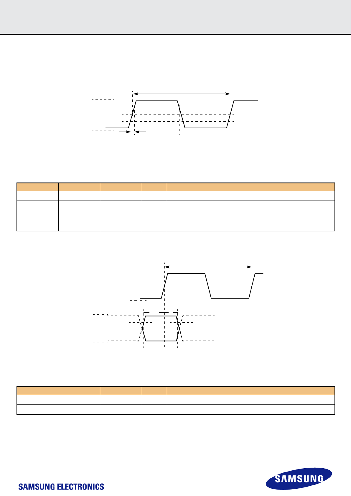
Host CLK Timing in HS200 mode shall conform to the timing specified in Figure 7 and Table 37. CLK input shall satisfy the clock timing over all possible
operation and environment conditions.CLK input parameters should be measured while CMD and DAT lines are stable high or low, as close as possible
to the Device. The maximum frequency of HS200 is 200MHz. Hosts can use any frequency up to the maximum that HS200 mode allows.
Figure 7. HS200 Clock signal timing
NOTE : 1. V
IH
denote V
IH
(min.) and V
IL
denotes V
IL
(max.).
2. V
T
=0.975V - Clock Threshold, indicates clock reference point for timing measurements.
[Table 36] HS200 Clock signal timing
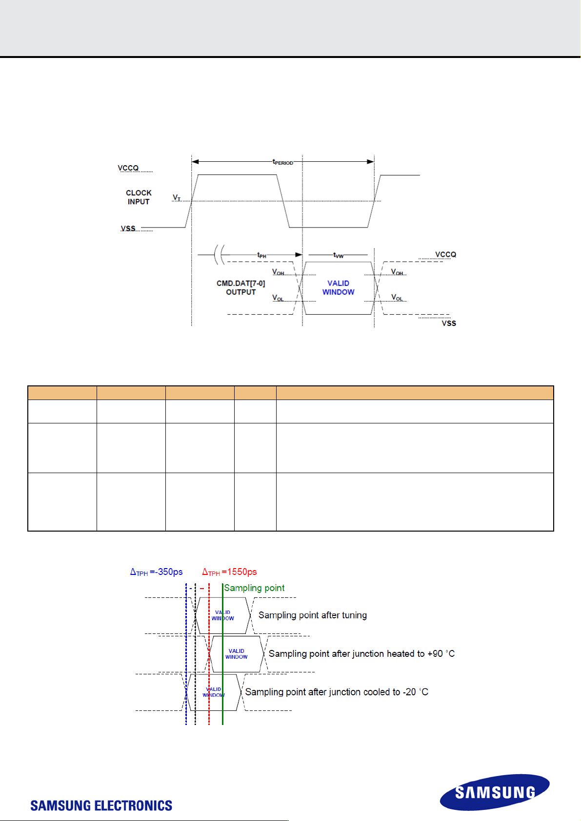
7.3.2 HS200 Device Input Timing
Figure 8. HS200 Device input timing
NOTE : 1. t
ISU
and t
IH
are measured at V
IL
(max.) and V
IH
(min.).
2. V
IH
denote V
IH
(min.) and V
IL
denotes V
IL
(max.).
[Table 37] HS200 Device input timing
symbol Min. Max. Unit Remark
t
PERIOD
5 - ns 200MHz (Max.), between rising edges
t
TLH
, t
THL
0.2 * t
PERIOD
ns
t
TLH
, t
THL
< 1ns (max.) at 200MHz,
C
BGA
= 12pF, The absolute maximum value of
t
TLH
, t
THL
is 10ns regatdless of clock frequency
Duty Cycle 30 70 %
Symbol Min. Max. Unit Remark
t
ISU
1.40 - ns
5pF≤C
BGA
≤ 12 pF
t
IH
0.8 ns
5pF≤C
BGA
≤12pF
t
TLH
t
THL
t
PERIOD
V
IH
V
T
V
IL
VCCQ
VSS
CLOCK
INPUT
VALID
WINDOW
V
IL
V
IH
t
IH
t
ISU
V
IL
V
IH
VCCQ
VSS
CMD.DAT[7-0]
INPUT
t
PERIOD
CLOCK
INPUT
V
T
VCCQ
VSS
- 27 -
IF THERE IS ANY OTHER OPERATION TO IMPLEMENT IN ADDITION TO SPECIFICATION
IN THE DATASHEET OR JEDEC STANDARD, PLEASE CONTACT EACH BRANCH OFFICE OR
HEADQUARTERS OF SAMSUNG ELECTRONICS.
datasheet
e·MMC
Rev. 1.0
KLMxGxGEAC-B001
SAMSUNG CONFIDENTIAL
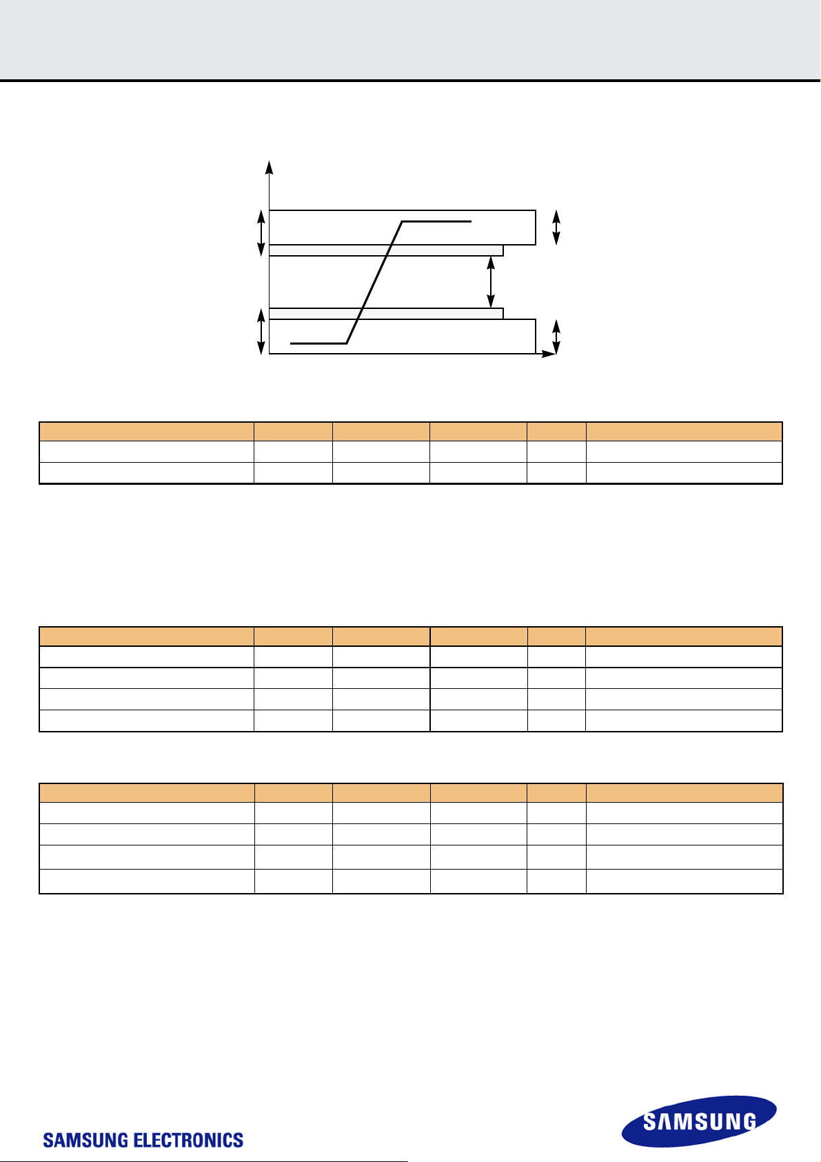
7.3.3 HS200 Device Output Timing
t
PH
parameter is defined to allow device output delay to be longer than t
PERIOD
. After initialization, the t
PH
may have random phase relation to the clock.
The Host is responsible to find the optimal sampling point for the Device outputs, while switching to the HS200 mode.
Figure 9 and Figure 38 define Device output timing. While setting the sampling point of data, a long term drift, which mainly depends on temperature
drift, should be considered. The temperature drift is expressed by Δ
TPH
. Output valid data window (t
VW
) is available regardless of the drift (Δ
TPH
) but
position of data window varies by the drift, as describes in Figure 10 .
Figure 9. HS200 Device output timing
NOTE: V
OH
denotes V
OH
(min.) and V
OL
denotes V
OL
(max.).
[Table 38] Output timing
NOTE: Unit Interval (UI) is one bit nominal time. For example, UI=5ns at 200MHz.
Figure 10. Δ
TPH
consideration
Symbol Min. Max. Unit Remark
tPH 0 2 UI
Device output momentary phase from CLK input to CMD or DAT lines output.
Does not include a long term temperature drift.
Δ
TPH
-350
(ΔT=-20 deg.C)
+1550
(ΔT=90 deg.C)
ps
Delay variation due to temperature change after tuning.
Total allowable shift of output valid window (T
VW
) from last system Tuning
procedure
Δ
TPH
is 2600ps for ΔT from -25 deg.C to 125 deg.C during operation.
t
VW
0.575 - UI
t
VW
=2.88ns at 200MHz
Using test circuit in Figure 13 including skew among CMD and DAT lines
created by the Device.
Host path may add Signal Integrity induced noise, skews, etc. Expected T
VW
at
Host input is larger than 0.475UI.
- 28 -
IF THERE IS ANY OTHER OPERATION TO IMPLEMENT IN ADDITION TO SPECIFICATION
IN THE DATASHEET OR JEDEC STANDARD, PLEASE CONTACT EACH BRANCH OFFICE OR
HEADQUARTERS OF SAMSUNG ELECTRONICS.
datasheet
e·MMC
Rev. 1.0
KLMxGxGEAC-B001
SAMSUNG CONFIDENTIAL
7.4 Bus signal levels
As the bus can be supplied with a variable supply voltage, all signal levels are related to the supply voltage.
7.4.1 Open-drain mode bus signal level
[Table 39] Open-drain bus signal level
NOTE:
1) Because Voh depends on external resistance value (including outside the package), this value does not apply as device specification.
Host is responsible to choose the external pull-up and open drain resistance value to meet Voh Min value.
7.4.2 Push-pull mode bus signal level eMMC
The device input and output voltages shall be within following specified ranges for any V
DD
of the allowed voltage range.
[Table 40] Push-pull signal level— high-voltage eMMC
[Table 41] Push-pull signal level— 1.70-1.95 V
CCQ
voltage Range
NOTE:
1) 0.7*V
DD
for MMC4.3 and older revisions.
2) 0.3*V
DD
for MMC4.3 and older revisions.
Parameter Symbol Min Max. Unit Conditions
Output HIGH voltage
V
OH
V
DD
- 0.2
V Note 1)
Output LOW voltage
V
OL
0.3 V
I
OL
= 2 mA
Parameter Symbol Min Max. Unit Conditions
Output HIGH voltage
V
OH
0.75*V
DD
V
I
OH
= -100 uA@V
DD
min
Output LOW voltage
V
OL
0.125*V
DD
V
I
OL
= 100 uA@V
DD
min
Input HIGH voltage
V
IH
0.625*V
DD
V
DD
+ 0.3
V
Input LOW voltage
V
IL
V
SS
- 0.3 0.25*V
DD
V
Parameter Symbol Min Max. Unit Conditions
Output HIGH voltage
V
OH
V
DD
- 0.45V
V
I
OH
= -2mA
Output LOW voltage
V
OL
0.45V V
I
OL
= 2mA
Input HIGH voltage
V
IH
0.65*V
DD
1)
V
DD
+ 0.3
V
Input LOW voltage
V
IL
V
SS
- 0.3
0.35*V
DD
2)
V
V
t
input
high level
input
low level
output
high level
output
low level
undefined
V
DD
V
IH
V
OH
V
IL
V
SS
V
OL