SYSTEMS-8030277-REV_C.pdf - 第21页
Enables smar ter and faster inspe ct ion • Reduce t raini ng eorts and minimi ze operat or int eraction sa ving ti me and co st with the po werful yet sim ple soft ware with in tuit ive m ulti-t ouch in ter face and 3 D…
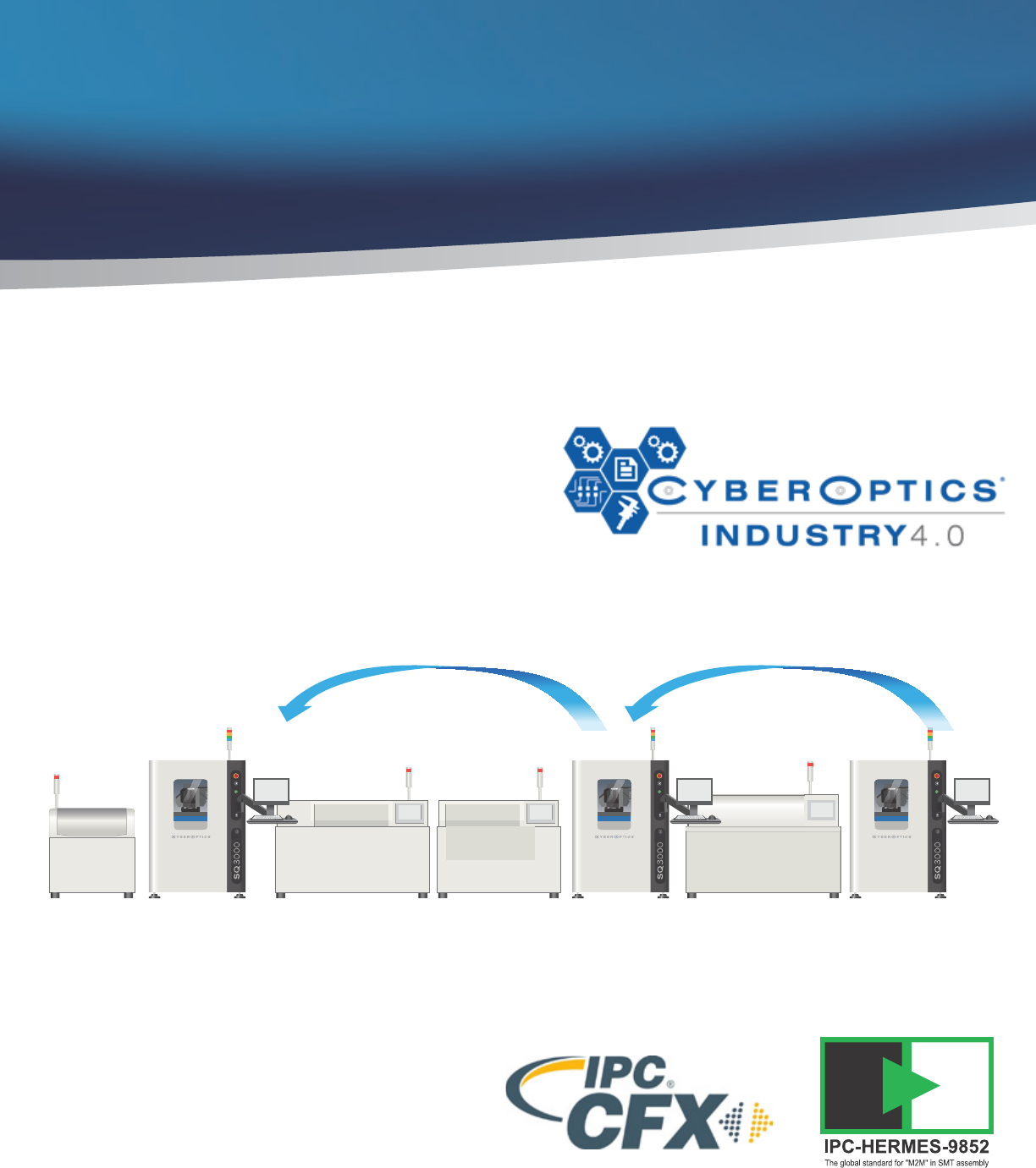
Industry 4.0
Intelligent Self-Learning, Self-Adjusting Zero Defect Line
Smart Factory Solution
CyberOptics oers a range of unique value-add software
solutions that enable automation, reduce rework costs, minimize
scrap and optimize print process.
CyberOptics Software Solutions provides our customers and
partners the best added-value possible for inspection and
measurement in electronics manufacturing.
Save Time, Save Expense and Improve Yields with
CyberOptics’ Powerful Value-Add Solutions
SPI Pre Reow AOI Post Reow AOI
As members and participants in the IPC-Connected
Factory Initiative and The Hermes Standard, CyberOptics
is committed to advancing machine-to-machine
communication in SMT assembly and maximize line
throughput and traceability in an open protocol.
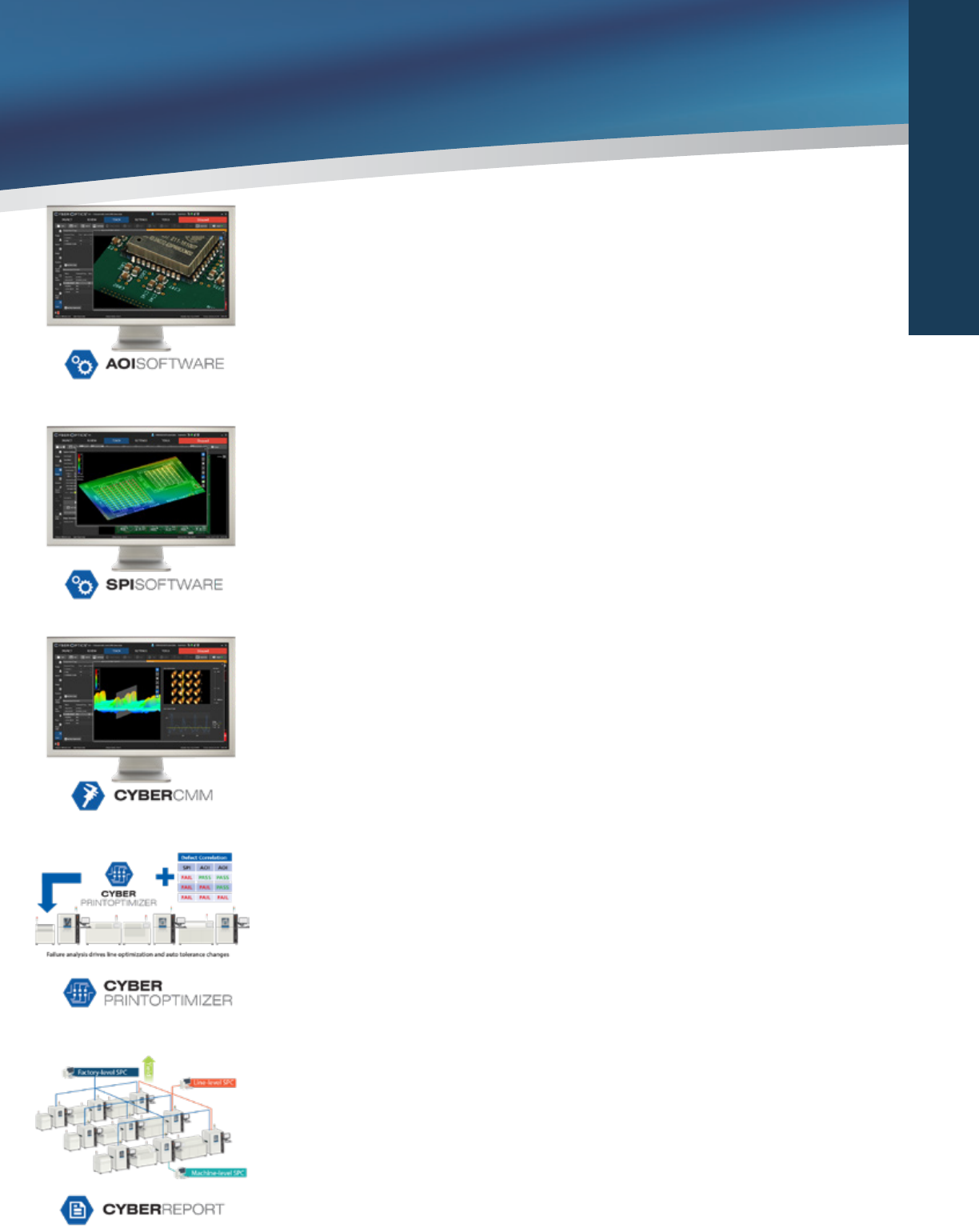
Enables smarter and faster inspection
• Reduce training eorts and minimize operator interaction saving time and cost
with the powerful yet simple software with intuitive multi-touch interface and 3D
visualization tools.
• Optimize printing process, establish stencil cleaning cycles and ne-tune printer set-up.
• Gain the power to do more with SPI results with closed loop feedback.
• Improve the solderability of smaller components by using the printing oset data for
compensating parts placement with forward capability.
Automatically optimizes the print process by proactively analyzing
current trend data.
• Improve yields and reduce downtime with its predictive process improvement
capability.
• Get started quickly with pre-dened templates
• Customize with customizable rules for specic product needs.
Enables smarter and faster inspection
• Ultra-fast programming capabilities, auto tuning and enhancements that
signicantly speed setup, simplify the process, reduce training eorts and
minimize operator interaction.
• Speed programming and performance with AI (Autonomous Image
Interpretation) technology for set-up in <13 minutes with a data-rich, pre-
loaded library and automated scripts that collect and update models all on their
own.
A complete Statistical Process Control (SPC), oers full-edged
machine-level to factory-level SPC capability to improves yields
• Attain eective process verication and control with traceability.
• Identify trends and enhance line yields with real-time monitoring tools for historical
analysis and reporting.
• Reduce training with easy-to-set-up intuitive interface that facilitates quick learning.
• Achieve fast parsing and charting speed with the robust and scalable software, while
enabling an extremely compact database size.
Enables smarter and faster coordinate measurement (Add-on)
• Extensive suite of CMM tools for precise measurement of critical features
• Signicantly speed measurements compared to traditional CMM systems, with high
accuracy and repeatability
• Multi-process capable – 3D AOI, 3D AOM, 3D CMM
INDUSTRY 4.0
Wafer-Level & Advanced Packaging
Metrology and Inspection Systems
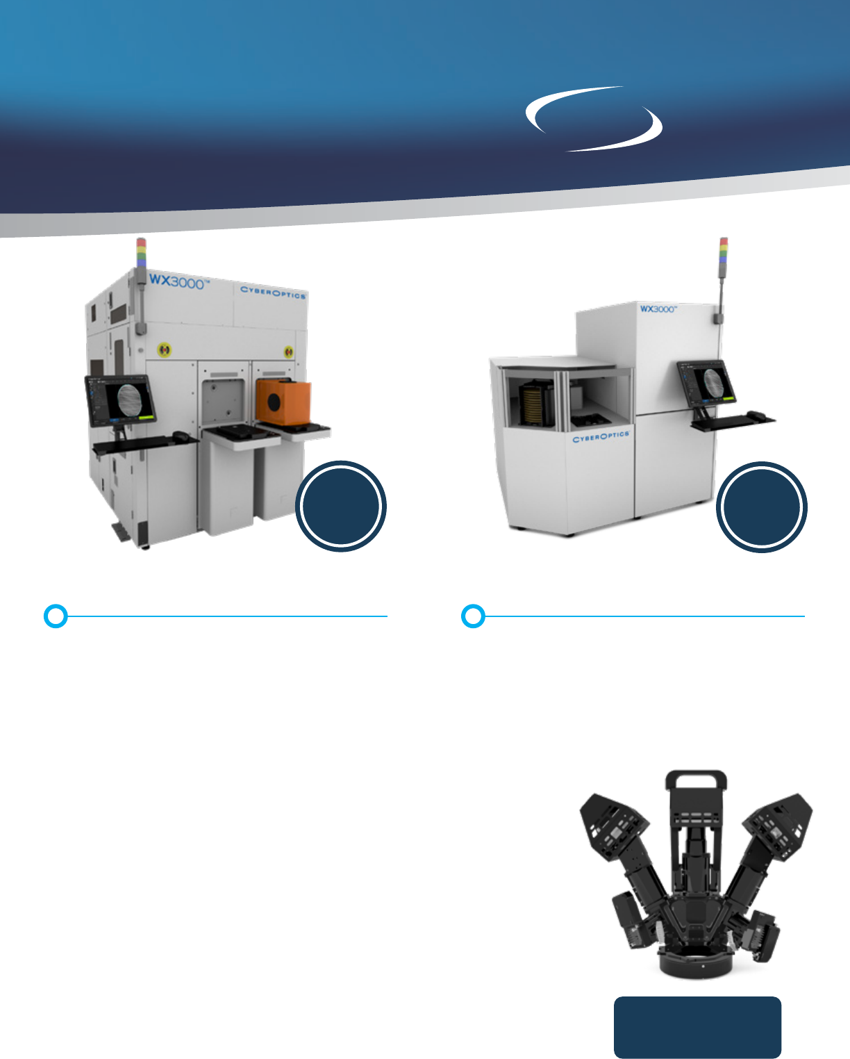
WX3000™
|
12” and 8” Wafer
3D+2D Metrology and Inspection
• Delivering metrology grade accuracy at
production speed, powered by NanoResolution
MRS Sensor Technology
• 12” and 8” wafer sizes
• Delivers throughput of 25 wafers (300mm)
per hour
Powered by NanoResolution Multi-Reection
Suppression (MRS) Sensor Technology
WX3000 3D and 2D metrology and inspection system provides the ultimate
combination of high speed, high resolution and high accuracy for wafer-level and
advanced packaging applications to improve yields and productivity. Oering an
unparalleled combination of high accuracy, high resolution and speed, MRS sensors
are widely used for inspection and measurement in the SMT and semiconductor
markets.
Proprietary MRS sensor technology, deemed best-in-class, meticulously identies
and rejects multiple reections caused by shiny components and mirror-like surfaces.
Eective suppression of multiple reections is critical for highly accurate measurements.
The 3-micron NanoResolution (X/Y resolution of 3 micron, Z resolution of 50 nanometer)
MRS sensor enables metrology grade accuracy with superior 100% 3D and 2D
measurement performance for features as small as 25-micron.
Powered by
MRS™ Technology
WX3000™
|
8” and 6” Wafer
3D+2D Metrology and Inspection
• Delivering metrology grade accuracy at
production speed, powered by NanoResolution
MRS Sensor Technology
• 8” and 6” wafer sizes
• Delivers throughput of 55 wafers (200mm)
per hour
12” and 8”
Wafer
Size
8” and 6”
Wafer
Size
NanoResolution
MRS Sensor