SYSTEMS-8030277-REV_C.pdf - 第22页
W afer- Le v e l & Advanc e d Pa ck aging Metrology and Ins pe c tion S ystem s WX3 000 ™ | 1 2” and 8” W afer 3D + 2D Met rol ogy an d In spec ti on • Delive ring metrol ogy grade acc uracy at production speed, powe…
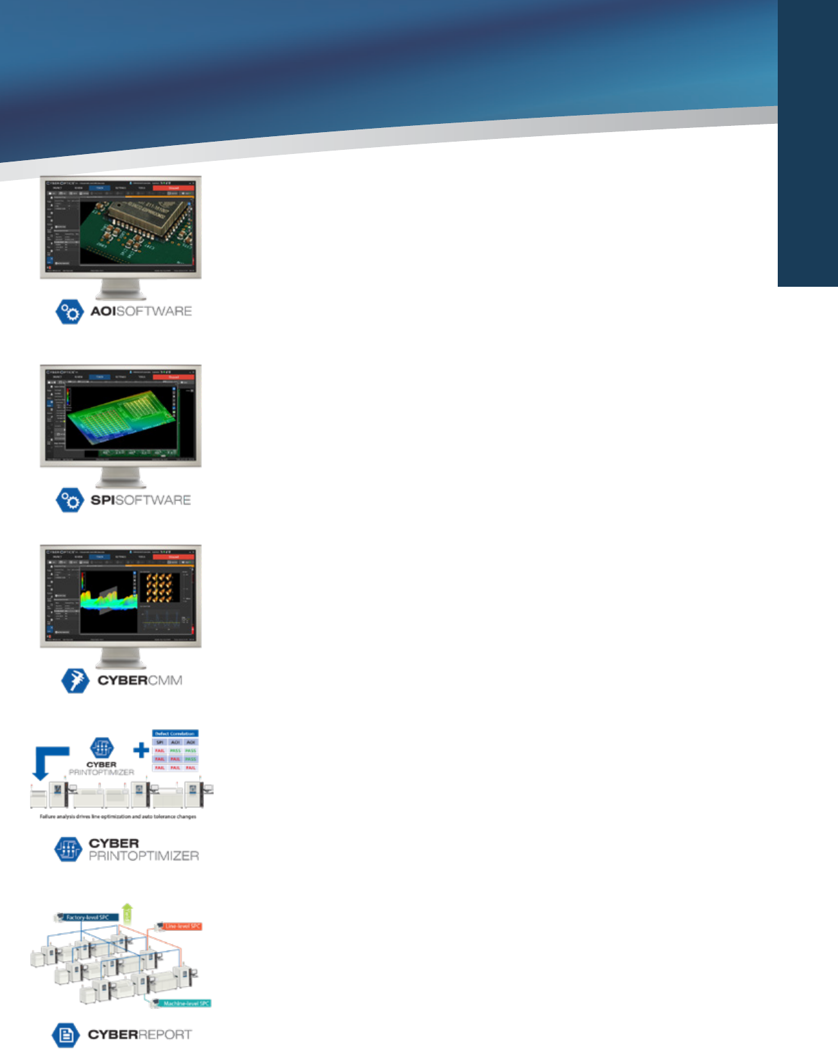
Enables smarter and faster inspection
• Reduce training eorts and minimize operator interaction saving time and cost
with the powerful yet simple software with intuitive multi-touch interface and 3D
visualization tools.
• Optimize printing process, establish stencil cleaning cycles and ne-tune printer set-up.
• Gain the power to do more with SPI results with closed loop feedback.
• Improve the solderability of smaller components by using the printing oset data for
compensating parts placement with forward capability.
Automatically optimizes the print process by proactively analyzing
current trend data.
• Improve yields and reduce downtime with its predictive process improvement
capability.
• Get started quickly with pre-dened templates
• Customize with customizable rules for specic product needs.
Enables smarter and faster inspection
• Ultra-fast programming capabilities, auto tuning and enhancements that
signicantly speed setup, simplify the process, reduce training eorts and
minimize operator interaction.
• Speed programming and performance with AI (Autonomous Image
Interpretation) technology for set-up in <13 minutes with a data-rich, pre-
loaded library and automated scripts that collect and update models all on their
own.
A complete Statistical Process Control (SPC), oers full-edged
machine-level to factory-level SPC capability to improves yields
• Attain eective process verication and control with traceability.
• Identify trends and enhance line yields with real-time monitoring tools for historical
analysis and reporting.
• Reduce training with easy-to-set-up intuitive interface that facilitates quick learning.
• Achieve fast parsing and charting speed with the robust and scalable software, while
enabling an extremely compact database size.
Enables smarter and faster coordinate measurement (Add-on)
• Extensive suite of CMM tools for precise measurement of critical features
• Signicantly speed measurements compared to traditional CMM systems, with high
accuracy and repeatability
• Multi-process capable – 3D AOI, 3D AOM, 3D CMM
INDUSTRY 4.0
Wafer-Level & Advanced Packaging
Metrology and Inspection Systems
WX3000™
|
12” and 8” Wafer
3D+2D Metrology and Inspection
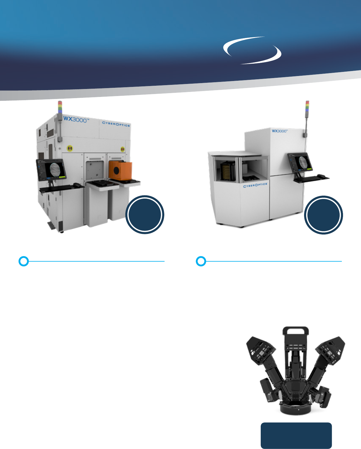
• Delivering metrology grade accuracy at
production speed, powered by NanoResolution
MRS Sensor Technology
• 12” and 8” wafer sizes
• Delivers throughput of 25 wafers (300mm)
per hour
Powered by NanoResolution Multi-Reection
Suppression (MRS) Sensor Technology
WX3000 3D and 2D metrology and inspection system provides the ultimate
combination of high speed, high resolution and high accuracy for wafer-level and
advanced packaging applications to improve yields and productivity. Oering an
unparalleled combination of high accuracy, high resolution and speed, MRS sensors
are widely used for inspection and measurement in the SMT and semiconductor
markets.
Proprietary MRS sensor technology, deemed best-in-class, meticulously identies
and rejects multiple reections caused by shiny components and mirror-like surfaces.
Eective suppression of multiple reections is critical for highly accurate measurements.
The 3-micron NanoResolution (X/Y resolution of 3 micron, Z resolution of 50 nanometer)
MRS sensor enables metrology grade accuracy with superior 100% 3D and 2D
measurement performance for features as small as 25-micron.
Powered by
MRS™ Technology
WX3000™
|
8” and 6” Wafer
3D+2D Metrology and Inspection
• Delivering metrology grade accuracy at
production speed, powered by NanoResolution
MRS Sensor Technology
• 8” and 6” wafer sizes
• Delivers throughput of 55 wafers (200mm)
per hour
12” and 8”
Wafer
Size
8” and 6”
Wafer
Size
NanoResolution
MRS Sensor
SEMI SYSTEMS
Fast, Superior Inspection Performance
Performing two to three times faster than alternate technologies at
data processing speeds in excess of 75 million 3D points per second,
the NanoResolution MRS Sensor delivers throughput greater than 25
wafers (300mm) per hour. 100% 3D and 2D metrology and inspection
can be completed simultaneously at high speed, versus an alternate,
slow method that requires two separate scans for 2D and 3D, and only
a sampling of a few die.
Versatility for Wafer-Level and Advanced Packaging Applications
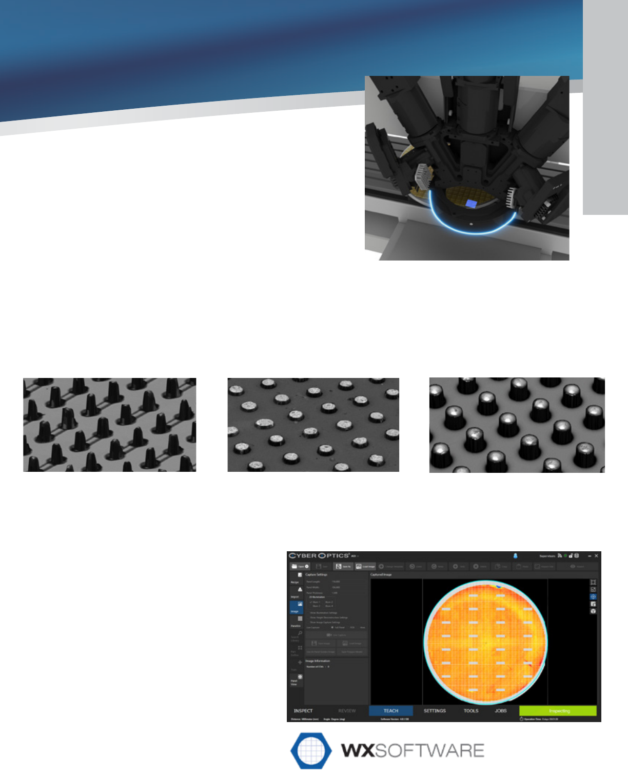
Measure and inspect a wide range of semiconductor applications including gold bumps, solder balls and bumps,
wafer bumps, copper pillars and other wafer-level and advanced packaging applications. Measure and inspect
critical packaging features including bump height, coplanarity, diameter and shape, relative location and variety of
other measurements.
Benets of 100% Wafer Bump
Metrology and Inspection
The WX3000 enables 100% 3D metrology and
inspection for wafer bumps that can identify:
• Cluster Defect, indication of equipment or process
issue
• Repeating Defect, potentially mask/ reticle defect
• Bump Height Distribution of Each Wafer, identify
performance dierences between dierent plating
machines and individual plating cells
• Non-uniform Bump Heights, indication of uneven
current density distribution of the plater
• Wafer Edge Tall Bumps, avoid probe card damage
Flip Chip (c4)Micro BumpCopper Pillar