SYSTEMS-8030277-REV_C.pdf - 第23页
SEMI SY STEMS F ast , Superior Insp ec tion Performance Pe r forming two to t hree ti mes faster t han al terna te t echnologi es at data proc ess ing s peeds in exce ss of 7 5 mill ion 3D poi nts per second, the NanoRes…
Wafer-Level & Advanced Packaging
Metrology and Inspection Systems
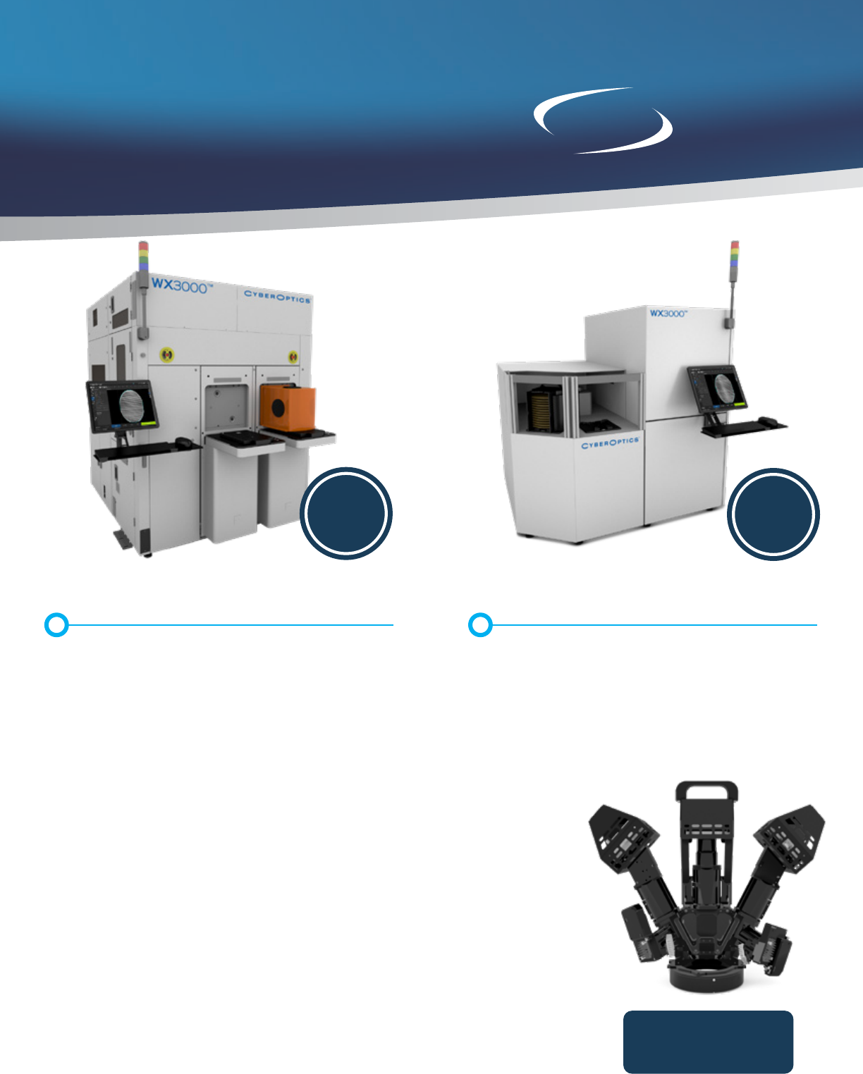
WX3000™
|
12” and 8” Wafer
3D+2D Metrology and Inspection
• Delivering metrology grade accuracy at
production speed, powered by NanoResolution
MRS Sensor Technology
• 12” and 8” wafer sizes
• Delivers throughput of 25 wafers (300mm)
per hour
Powered by NanoResolution Multi-Reection
Suppression (MRS) Sensor Technology
WX3000 3D and 2D metrology and inspection system provides the ultimate
combination of high speed, high resolution and high accuracy for wafer-level and
advanced packaging applications to improve yields and productivity. Oering an
unparalleled combination of high accuracy, high resolution and speed, MRS sensors
are widely used for inspection and measurement in the SMT and semiconductor
markets.
Proprietary MRS sensor technology, deemed best-in-class, meticulously identies
and rejects multiple reections caused by shiny components and mirror-like surfaces.
Eective suppression of multiple reections is critical for highly accurate measurements.
The 3-micron NanoResolution (X/Y resolution of 3 micron, Z resolution of 50 nanometer)
MRS sensor enables metrology grade accuracy with superior 100% 3D and 2D
measurement performance for features as small as 25-micron.
Powered by
MRS™ Technology
WX3000™
|
8” and 6” Wafer
3D+2D Metrology and Inspection
• Delivering metrology grade accuracy at
production speed, powered by NanoResolution
MRS Sensor Technology
• 8” and 6” wafer sizes
• Delivers throughput of 55 wafers (200mm)
per hour
12” and 8”
Wafer
Size
8” and 6”
Wafer
Size
NanoResolution
MRS Sensor
SEMI SYSTEMS
Fast, Superior Inspection Performance
Performing two to three times faster than alternate technologies at
data processing speeds in excess of 75 million 3D points per second,
the NanoResolution MRS Sensor delivers throughput greater than 25
wafers (300mm) per hour. 100% 3D and 2D metrology and inspection
can be completed simultaneously at high speed, versus an alternate,
slow method that requires two separate scans for 2D and 3D, and only
a sampling of a few die.
Versatility for Wafer-Level and Advanced Packaging Applications
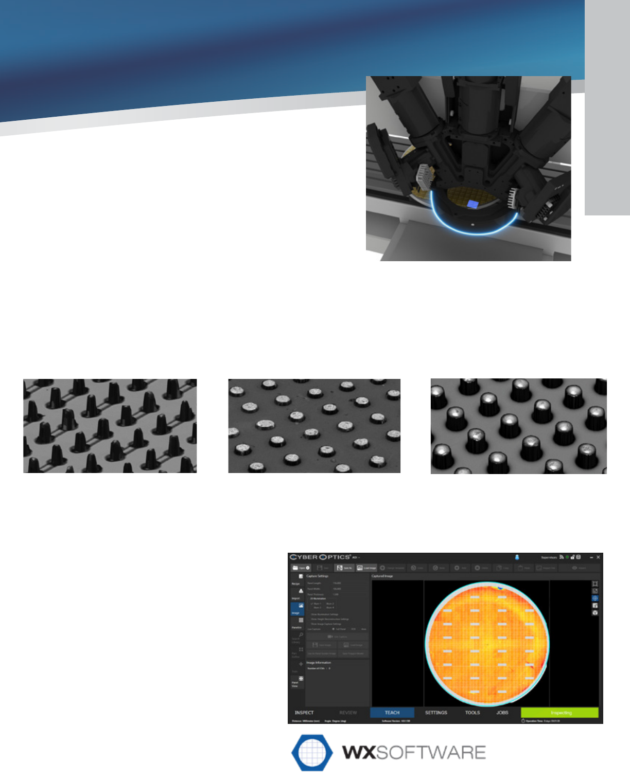
Measure and inspect a wide range of semiconductor applications including gold bumps, solder balls and bumps,
wafer bumps, copper pillars and other wafer-level and advanced packaging applications. Measure and inspect
critical packaging features including bump height, coplanarity, diameter and shape, relative location and variety of
other measurements.
Benets of 100% Wafer Bump
Metrology and Inspection
The WX3000 enables 100% 3D metrology and
inspection for wafer bumps that can identify:
• Cluster Defect, indication of equipment or process
issue
• Repeating Defect, potentially mask/ reticle defect
• Bump Height Distribution of Each Wafer, identify
performance dierences between dierent plating
machines and individual plating cells
• Non-uniform Bump Heights, indication of uneven
current density distribution of the plater
• Wafer Edge Tall Bumps, avoid probe card damage
Flip Chip (c4)Micro BumpCopper Pillar

Contact CyberOptics today for more information
+1 800.366.9131 or +1 763.542.5000 | CSsales@cyberoptics.com | www.cyberoptics.com
Copyright © Nordson Corporation. All rights reserved. Specications subject to change without notice. 8030277 Rev C
CyberOptics Corporation is a leading global developer and manufacturer of high-precision
3D sensing technology solutions. CyberOptics’ sensors are used for inspection and metrology in the
SMT and semiconductor capital equipment markets to signicantly improve yields and productivity.
By leveraging its leading edge technologies, the Company has strategically established itself as a
global leader in high precision 3D sensors, allowing CyberOptics to further increase its penetration of
key vertical markets.
Headquartered in Minneapolis, Minnesota, CyberOptics conducts worldwide operations through
its facilities in North America, Asia and Europe. Through continuous technology advancements, a
rich patent portfolio, and our sensor expertise CyberOptics continues to be an industry leader at the
forefront of technology.