IPC 7711A.pdf - 第223页
OUTLINE This procedure is used to repair minor damage to printed wiring board base mate- rial. Scrapes and scratches in the board base material may be caused by accidents during handling. Burns in the base material may b…
6. Install an end mill into the chuck of the drill press. Machine a tongue onto both
sides of the replacement piece. The dimensions of the tongue should match the
size of the milled groove. (See Figure 3.)
7. Where required apply tape to protect exposed parts of printed wiring board
bordering the prepared area.
8. Carefully check the fit of the replacement piece and then clean both the replace-
ment piece and the slot. The replacement base material should fit firmly into the
slot so that it will not move or fall out when epoxied in place.
9. Apply tape to the surface of the printed wiring board adjacent to the slot. The
tape should protect any adjacent contacts or components.
10. Mix the epoxy.
11. Apply a small amount of epoxy to the edges of the replacement piece and to
the inside edges of the slot.
12. Insert the replacement piece into the slot. Check alignment. Remove excess
epoxy. (See Figure 4.)
13. If needed, apply additional epoxy to the edges of the slot. A wood stick sharp-
ened at the end may be used to apply the epoxy.
14. Cure the epoxy per the manufacturers instructions.
CAUTION
Some components may be sensitive to high temperature.
15. After the epoxy has cured remove the tape.
16. If needed use the knife or scraper and scrape off any excess epoxy.
NOTE
If needed, apply additional thin coating to seal any scrapped areas.
17. Clean the area.
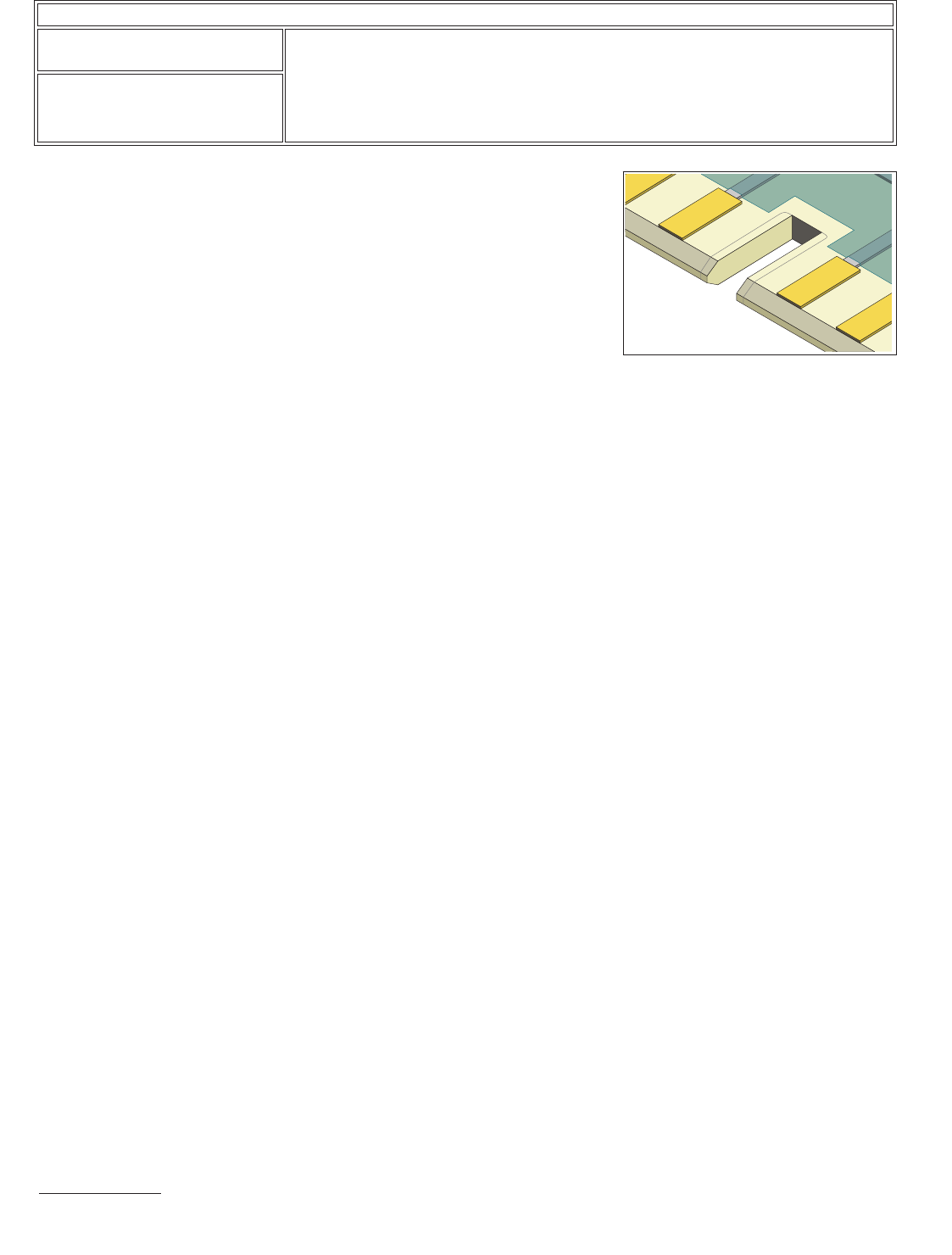
18. Cut off excess length of replacement material and file to match contour of exist-
ing edge. (See Figure 5.)
19. If a new slot is needed, machine using milling machine and appropriate milling
cutter. Use great care to correctly relocate the slot.
20. Clean the area.
EVALUATION
1. Visual examination and measurement of key slot location and dimension.
NOTES
Figure 5 Cut off excess material and
file to match edge.
IPC-7721A
Number: 3.4.2
Revision:
Date: 2/98
Subject: Key and Slot Repair, Transplant Method
Page2of2
Copyright Association Connecting Electronics Industries
Provided by IHS under license with IPC
Not for Resale
No reproduction or networking permitted without license from IHS
--``,``,-`-`,,`,,`,`,,`---
OUTLINE
This procedure is used to repair minor damage to printed wiring board base mate-
rial. Scrapes and scratches in the board base material may be caused by accidents
during handling. Burns in the base material may be caused by improper use of sol-
dering and desoldering tools.
CAUTION
This method may be used when the damage extends deep into the base material,
but not completely through. If the base board material is damaged completely
through, see Procedure No. 3.5.2 or 3.5.3.
CAUTION
Surface conductors may need to be replaced in the damaged area. Be sure that the
appropriate conductor diagrams, or photographs reflecting the original conductors
are available so that they may be replaced after repairing the base board material.
Damage to internal conductors or planes may have to be restored using surface
wires.
REFERENCES
2.1 Handling Electronic Assemblies
2.2 Cleaning
2.5 Baking and Preheating
2.6 Epoxy Mixing and Handling
TOOLS & MATERIALS
Ball Mills, Carbide
Cleaner
Color Agent,
Various Colors
Epoxy
Hand Held Drill
Halogen Light
Heat Lamp
Polyimide Tape
Knife
Microscope
Oven
Scraper
Wipes
PROCEDURE
1. Clean the damaged area.
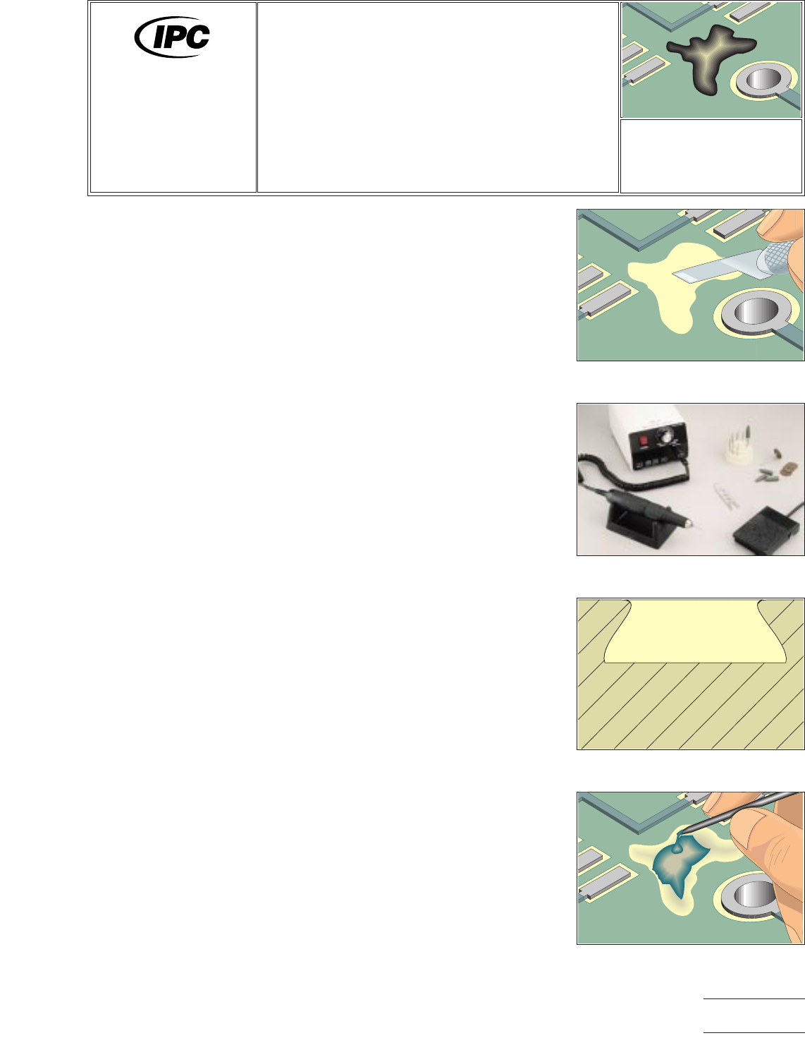
2. Scrape away the damaged board base material using a knife.
All damaged base board material and solder resist must be removed at the sur-
face. (See Figure 1.) See step 2A for alternate method.
NOTE
To clearly see that all damaged material has been removed, flood the area with
alcohol or solvent. Damaged internal fibers of the base material will show up
clearly.
Figure 1 Scrape away damaged base
board material with a knife.
Figure 2 Commercially available hand
held drill.
Figure 3 An undercut to enhance
mechanical strength.
Figure 4 Apply the epoxy with a wood
stick sharpened at the end.
7721A
Repair and
Modification of
Printed Boards and
Electronic Assemblies
Revision:
Date: 2/98
Base Material Repair,
Epoxy Method
Number: 3.5.1
Product Class: R, W
Skill Level: Advanced
Level of Conformance: High
Material in this manual was voluntarily established by Technical Committees of IPC. This material is advisory only and its use
or adaptation is entirely voluntary. IPC disclaims all liability of any kind as to the use, application, or adaptation of this material.
Users are also wholly responsible for protecting themselves against all claims or liabilities for patent infringement. Equipment
referenced is for the convenience of the user and does not imply endorsement by IPC.
Page1of2
Copyright Association Connecting Electronics Industries
Provided by IHS under license with IPC
Not for Resale
No reproduction or networking permitted without license from IHS
--``,``,-`-`,,`,,`,`,,`---
CAUTION
Abrasion operations can generate electrostatic charges.
2A. Mill away the damaged board base material using dental style drill and ball
mill. All damaged base board material and solder resist must be removed.
(See Figure 2.)
NOTE
An undercut to enhance mechanical strength may be desired for class 3
product. (See Figure 3.)
3. Remove all loose material and clean the area.
4. Where needed, apply tape to protect exposed parts of printed wiring board.
NOTE
The printed wiring board may be preheated prior to filling the area with epoxy.
A preheated printed wiring board will allow the epoxy to easily flow and level out.
Epoxy applied to an unheated printed wiring board may settle below the printed
wiring board surface as the epoxy cures.
5. Mix the epoxy. If desired, add color agent to the mixed epoxy to match the
printed wiring board color.
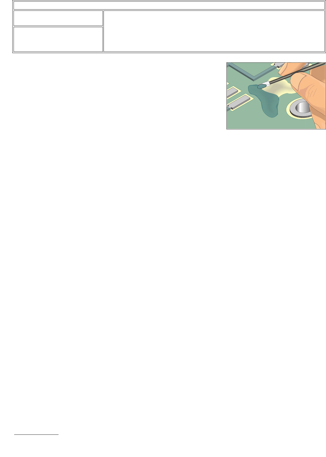
6. Fill the area with epoxy up to and flush with the printed wiring board surface. No
fibers of laminate material should be exposed. A wood stick sharpened at the
end may be used to apply and spread the epoxy. For large areas, apply the
epoxy with a foam swab to create a texture in the surface. (See Figures 4 and
5.)
NOTE
A slight overfill of epoxy may be desired to allow for shrinkage when epoxy
cures.
NOTE
Epoxy may be applied using a foam swab to restore the surface appearance.
7. Cure the epoxy per the manufacturer’s instructions.
CAUTION
Some components may be sensitive to high temperature.
8. After the epoxy has cured remove the tape.
9. If needed, use a knife or scraper and scrape off any excess epoxy. Scrape until
the new epoxy surface is level with the surrounding printed wiring board surface.
10. Remove all loose material. Clean the area.
NOTE
If needed, apply an additional thin coating to seal any scraped areas.
EVALUATION
1. Visual examination for texture and color match.
2. Electrical tests to conductors around the repaired area as applicable.
NOTES
Figure 5 Apply the epoxy with a foam
swab to create a texture in the surface.
IPC-7721A
Number: 3.5.1
Revision:
Date: 2/98
Subject: Base Material Repair, Epoxy Method
Page2of2
Copyright Association Connecting Electronics Industries
Provided by IHS under license with IPC
Not for Resale
No reproduction or networking permitted without license from IHS
--``,``,-`-`,,`,,`,`,,`---