IPC 7711A.pdf - 第287页
PREPARATION − Remove Poor Plating or Surface Defects 1. Clean the rework area. 2. Apply plating tape to the printed wiring board surface surrounding the area to be reworked. The plating tape will protect adjacent compone…
TOOLS & MATERIALS
Abrasive Pad
Board Support
Burnisher
Cleaner
Cleaner Wipes
Connector Edge
Plating System
Conductive Pen
Desoldering Braid or
Desoldering System
Eraser Stick
Gloves, Antistatic
Polyimide Tape
Knife
Liquid Flux
Peel Testing Tape
Pin Fixtures
Plating Anodes
Plating Cables
Plating Probe
Plating Solution, Gold
Plating Solution, Nickel
Plating Solution, Electroclean
Plating Solution, Solder Strip
Plating Tape
Power Supply
Probe Clip
Rinse Bottle
Rinse Tray
Safety Glasses
Solder
Solder Iron
Solution Cups
Solution Tray
Swab
Thickness Measuring System,
Gold and Nickel
Water/Air Sprayer
Wire, Buss, 30 AWG
Work Sink
PREPARATION − Remove Solder Contamination
CAUTION
Safety glasses and safety gloves should always be worn when handling hazardous
chemicals. Do not work within a small enclosed room without supplemental ventila-
tion. If ventilation is not adequate, use a fan to move fumes away from the operator.
1. Clean the rework area.
2. Apply plating tape to the printed wiring board surface surrounding the area to
be reworked. (See Figure 1.) The plating tape will protect adjacent components
and the printed wiring board surface from unwanted exposure to stripping and
plating solutions.
3. Flow solder over the entire area of any contacts that have contamination using
a soldering iron. This provides a more even surface when plating. Remove the
bulk of the solder contamination using desoldering tools or desoldering braid.
(See Figure 2.)
4. Clean the area.
5. Place the printed wiring board on the board support so that the leading edge
overhangs the rinse tray.
6. Swab the solder stripping solution over the solder contamination using a swab.
Swab the surface until all remaining solder has been stripped off. (See Figure 3.)
7. Thoroughly rinse the entire area with water. (See Figure 4.)
8. Mildly buff the contacts using abrasive pad. Mild buffing will prepare the surface
for plating and remove any remaining solder contamination.
9. Thoroughly rinse with water to remove any residue.
Figure 5 Solder a wire to the edge of
the contacts needing plating.
Figure 6 Apply conductive paint to
the edge of the contacts.
Figure 7 Sample plating anodes
shown with fabric wrapping.
Figure 8 Brush the surface with the
saturated plating probe.
IPC-7721A
Number: 4.6.3
Revision:
Date: 2/98
Subject: Edge Contact Repair, Plating Method
Page2of6
Copyright Association Connecting Electronics Industries
Provided by IHS under license with IPC
Not for Resale
No reproduction or networking permitted without license from IHS
--``,``,-`-`,,`,,`,`,,`---

PREPARATION − Remove Poor Plating or Surface Defects
1. Clean the rework area.
2. Apply plating tape to the printed wiring board surface surrounding the area to
be reworked. The plating tape will protect adjacent components and the printed
wiring board surface from unwanted exposure to stripping and plating solutions.
3. Clean the area.
4. Buff the contacts using an abrasive pad. Buff the contacts until all defective or
poor plating is removed.
5. Burnish small scratches. Use the tip of the burnisher to work the copper mate-
rial into the scratch and smooth out the area. Finish by mildly buffing the area to
remove any minor burnishing marks. If there are large scratches the contact
may need replacement. See Procedure Number 4.6.1 or 4.6.2.
6. Thoroughly rinse the entire area with water to remove any residue.
BUSSING
A conductive buss must be made to all the contacts that need plating. There are 4
basic connection options.
NOTE
Making a reliable buss connection is the most important step in plating. All sorts of
problems will be eliminated by taking the time to make a reliable buss connection.
BUSSING − Wire Soldered to Edge (Option 1)
CAUTION
When finished, this method will leave a small unplated line along the inner tip of each
contact.
1. Apply Polyimide tape to all the contacts to be plated. The tape should cover the
entire contact except for a small line along the inboard edge. The tape will pre-
vent further solder contamination.
2. Solder a wire directly to the inboard tip or connecting conductor of each con-
tact to be plated. The smallest amount of solder should be used to prevent fur-
ther contamination. (See Figure 5.)
BUSSING − Conductive Paint Applied to Edge (Option 2)
CAUTION
When finished, this method will leave a small unplated line along the inner tip of each
contact.
1. Apply Polyimide tape to all the contacts to be plated. The tape should cover the
entire contact except for a small line along the inboard edge. The tape will pre-
vent the conductive paint from contaminating the contact surface.
2. Apply a thin coating of conductive paint directly to the inboard tip of each con-
tact to be plated. The conductive paint should extend out to one edge so that
a clip can be applied to make electrical connection. (See Figure 6.)
IPC-7721A
Number: 4.6.3
Revision:
Date: 2/98
Subject: Edge Contact Repair, Plating Method
Page3of6
Copyright Association Connecting Electronics Industries
Provided by IHS under license with IPC
Not for Resale
No reproduction or networking permitted without license from IHS
--``,``,-`-`,,`,,`,`,,`---

BUSSING − Mechanical Probe, Individual Contacts (Option 3)
1. Each contact needing plating can be individually probed using the plating probe.
Touch the tip of the plating probe to the inboard edge of each contact or to the
connecting conductor as each solution is applied during the plating process.
BUSSING − Pin Fixture, Multiple Contacts (Option 4)
1. Make a mechanical connection to each contact using a pin fixture. The pin fix-
ture has spring loaded contact pins on centers matching the spacing of the
edge contacts to be plated. The contact pins make direct mechanical connec-
tion to the inboard tip of each contact, the connecting conductor trace or a
connecting plated through hole.
PROCEDURE − Plating Process
1. Place the printed wiring board on the board support so that the leading edge
overhangs the rinse tray.
2. Make the cathode connection (-) to the printed wiring board by using a plating
probe or probe clip. Connect the probe clip directly to the wire buss connection
or to the edge where conductive paint has been applied. The cable should be
connected to the (-) or black jack on the power supply.
3. Connect the plating probe to the power supply (+) or red jack. (See Figure 7.)
4. Set the output current on the power supply to setting recommended by the
equipment manufacturer.
5. Dip the plating probe into the electroclean plating solution. Wait a few seconds
for the solution to saturate the absorbent wrapping.
6. Swab the entire surface to be plated by brushing the surface with the saturated
plating probe. The plating probe should be moved back and forth briskly to pre-
vent burning and to provide even coverage. (See Figure 8.) Swab the area for
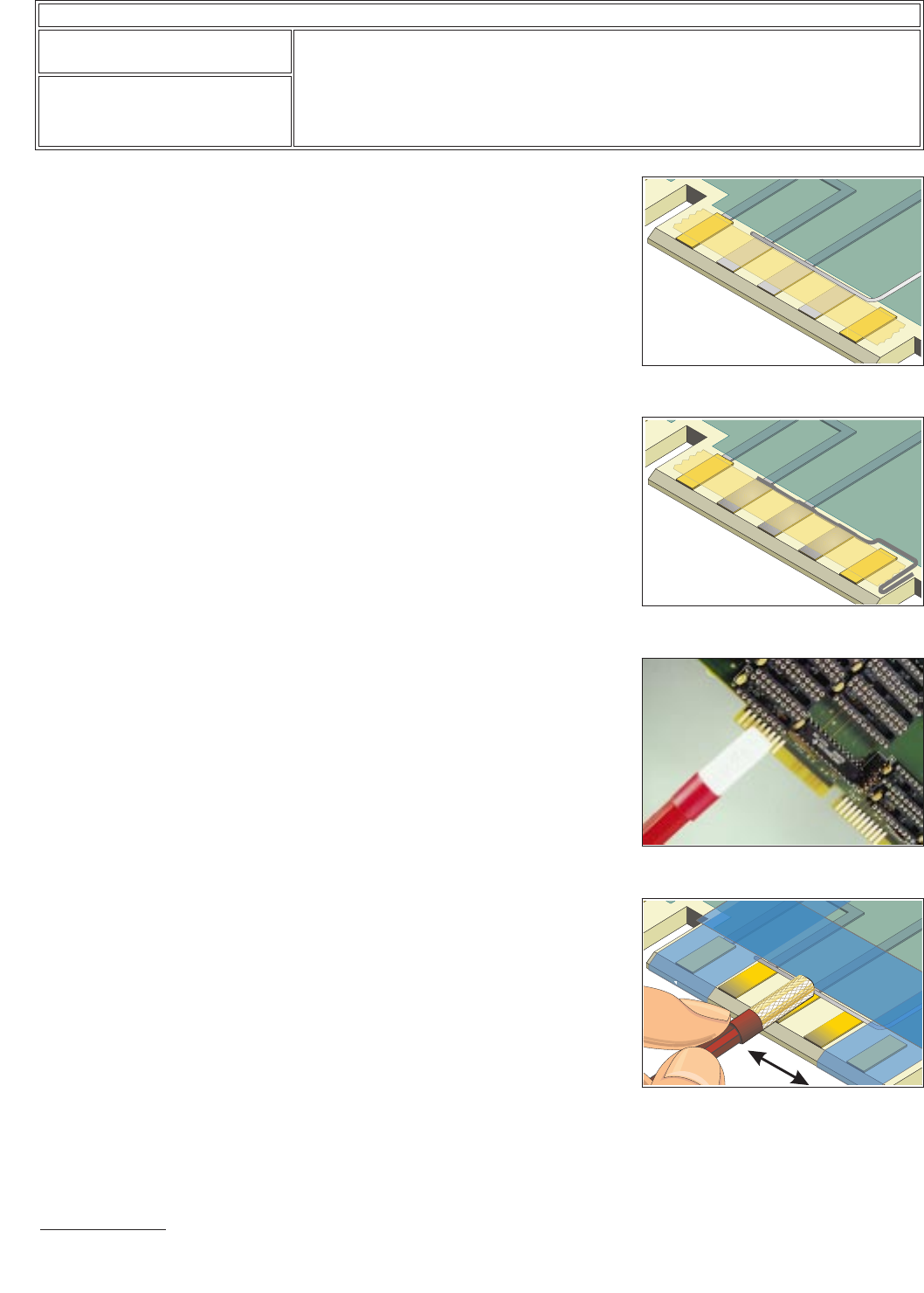
the time recommended by the equipment manufacturer.
7. Thoroughly rinse the entire area with water. Any burning or darkening of the
contacts may be removed with an abrasive pad. Saturate the abrasive pad and
the printed wiring board surface with water and lightly buff the contacts until all
evidence of the burning or discoloring is removed. Rinse the entire area with
water.
CAUTION
Do not allow the rework area to dry out between steps. The water coating pre-
vents oxidation.
8. Connect the nickel plating probe to the power supply (+) or red jack.
9. Dip the plating probe into the nickel plating solution. Wait a few seconds for the
solution to saturate the absorbent wrapping.
10. Swab the entire surface to be plated by brushing the surface with the saturated
plating probe. The plating probe should be moved back and forth briskly to pre-
vent burning and to provide even coverage. Swab the area for the time recom-
mended by the equipment manufacturer. Before rinsing, lightly buff the contacts
with an abrasive pad.
IPC-7721A
Number: 4.6.3
Revision:
Date: 2/98
Subject: Edge Contact Repair, Plating Method
Page4of6
Copyright Association Connecting Electronics Industries
Provided by IHS under license with IPC
Not for Resale
No reproduction or networking permitted without license from IHS
--``,``,-`-`,,`,,`,`,,`---