IPC 7711A.pdf - 第252页
2. Expose CAD generated additive conductor patterns of new conductor revision in isolation layer, copper and solder screens. 3 Print and cure isolation layer of protective epoxy. 4 Print, metalize and cure the new conduc…
OUTLINE
This modification/repair conductive pattern is fabricated via a solder/copper com-
posite of screen printable polymer thick film (PTF). The interconnects are established
at conductor lands and through hole locations of the original conductor. Electrical
continuity is optimized between two or more points of interconnection by solder
fusion of the new conductor pattern to the original etched PCB pattern.
NOTE
This modification/repair method is UL recognized, Type 1 94-V-0. It is compatible
with both digital and analog printed wiring board applications and it has resistance
of less than 3.0 milliohms/sq. It consists of greater than 90% copper and solder. The
resin system employed is thermal setting and adhesion of approximately 1.5 kg on
a 6 mm x 0.6 mm wide strip. It is typically applied to either or both sides of printed
wiring boards on thru-hole or surface mount PCB’s prior to assembly, without any
final solder resist coating. (Line resist coating can be applied and it is considered
optional.)
CAUTION
This modification/repair method can be employed on a single-sided, double-sided or
a multilayer printed wiring board. Its primary application is for signal carrying conduc-
tors. New or additional power distribution should be designed into the new conduc-
tor pattern on the basis of 0.25 mm of line width 2.6 amps of current required, up to
a maximum of 3.4 amps. When applying this method to the wave solder side or a
thru-hole printed wiring board, it should be covered with a solder (line) resist.
REFERENCES
2.1 Handling Electronic Assemblies
2.2 Cleaning
2.5 Baking and Preheating
TOOLS AND MATERIALS
Screen printer/screens with matalizer and IR belt ovens
Modification/repair master artwork
Conductive Ink, directly solderable
SMT compatible solder paste
IR solder reflow (fuse) belt oven
Flux cleaner, deionized water
Electronic multi-point tester
PROCEDURE
1. Convert conductor design revision via CAD to additive layer conductor pattern
including vias to be exposed and etch deletes to be performed.
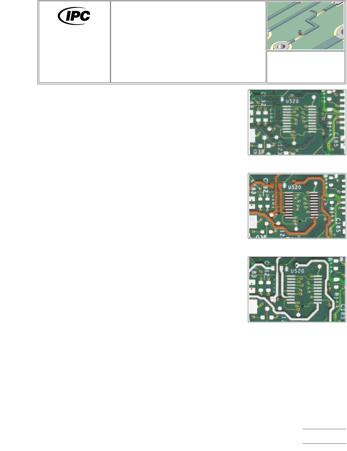
Figure 1 Isolation layer.
Figure 2 Copper ink is applied.
Figure 3 Solder ink fused to copper
ink.
7721A
Repair and
Modification of
Printed Boards and
Electronic Assemblies
Revision:
Date: 2/98
Conductor Repair/
Modification, Conductive
Ink Method
Number: 4.2.6
Product Class: R, F, C
Skill Level: Expert
Level of Conformance: Medium
Material in this manual was voluntarily established by Technical Committees of IPC. This material is advisory only and its use
or adaptation is entirely voluntary. IPC disclaims all liability of any kind as to the use, application, or adaptation of this material.
Users are also wholly responsible for protecting themselves against all claims or liabilities for patent infringement. Equipment
referenced is for the convenience of the user and does not imply endorsement by IPC.
Page1of2
Copyright Association Connecting Electronics Industries
Provided by IHS under license with IPC
Not for Resale
No reproduction or networking permitted without license from IHS
--``,``,-`-`,,`,,`,`,,`---

2. Expose CAD generated additive conductor patterns of new conductor revision
in isolation layer, copper and solder screens.
3 Print and cure isolation layer of protective epoxy.
4 Print, metalize and cure the new conductive ink pattern which establishes the
modified/repaired conductor.
5. Print the SMT compatible solder paste on to the cured conductive ink pattern,
totally encompassing the underlying material.
6 Fuse the printed solder paste to form the electrical optimization of the new con-
ductor and the interconnection to the original etched conductor. See reflow sol-
dering (IPC-J-STD-001).
CAUTION
Care should be taken not to add any solder to any unmodified or un-repaired areas
on the printed wiring board. All solder flux residue should be removed to meet IPC-
TM-650, Test Methods 2.3.25 and 2.3.26, ionic contamination requirements.
EVALUATION
Visually examine and conduct dimensional measurement of conductor width and
spacing. Ring-out for electrical continuity to detect for ‘shorts’ or ‘opens.’ This test-
ing can be affected manually via continuity meter, automated electronic point-to-
point tester or via a universal bed of nails electronic tester.
NOTE
Additive Conductor Modification Operations has become an industry standard for
production quantities of PCB modification/repair revisions.
NOTE
Because of the expert level of workmanship required, qualified vendors of the ser-
vice should be considered or the acquisition of dedicated in-house systems and
personnel to perform this work.
NOTES
IPC-7721A
Number: 4.2.6
Revision:
Date: 2/98
Subject: Conductor Repair/Modification, Conductive Ink Method
Page2of2
Copyright Association Connecting Electronics Industries
Provided by IHS under license with IPC
Not for Resale
No reproduction or networking permitted without license from IHS
--``,``,-`-`,,`,,`,`,,`---
OUTLINE
This method is used to replace damaged or missing conductors on internal layers of
multilayer printed wiring boards.
CAUTION
The conductor widths, spacing and current carrying capacity must not be reduced
below allowable tolerances.
CAUTION
The overlap joint used in this method may cause problems with high frequency cir-
cuitry.
CAUTION
This procedure is complicated and should be attempted only by properly skilled
repair personnel using the best tools and equipment.
REFERENCES
2.1 Handling Electronic Assemblies
2.2 Cleaning
2.5 Baking and Preheating
2.6 Epoxy Mixing and Handling
TOOLS AND MATERIALS
Ball Mills
Buffer
Conductor Foil Jumpers
Cleaner
Cleaning Wipes
Color Agent
Epoxy
Hand Held Drill
Heat Lamp
Polyimide Tape
Knife
Liquid Flux
Microscope
Oven
Scraper
Solder
Soldering Iron
PROCEDURE
1. Locate and determine the coordinates where the repair is to be made. Use films
or master drawings of the board as needed.
NOTE
Obtain as much information as possible on the conductive and non-conductive
layers prior to starting the procedure.
2. Remove components from the immediate area if necessary and clean the area.
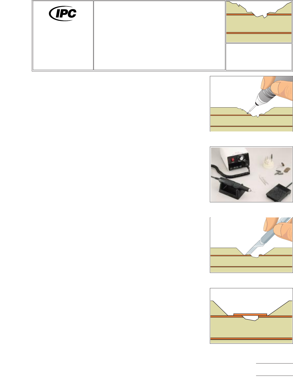
Figure 1 Milling into multilayer board
to expose the damaged conductors.
Figure 2 A high quality, hand held
drill.
Figure 3 Remove the remaining board
material with a knife.
Figure 4 Conductor foil jumper in
place ready to be soldered.
7721A
Repair and
Modification of
Printed Boards and
Electronic Assemblies
Revision:
Date: 2/98
Conductor Repair,
Inner Layer Method
Number: 4.2.7
Product Class: R, F
Skill Level: Expert
Level of Conformance: High
Material in this manual was voluntarily established by Technical Committees of IPC. This material is advisory only and its use
or adaptation is entirely voluntary. IPC disclaims all liability of any kind as to the use, application, or adaptation of this material.
Users are also wholly responsible for protecting themselves against all claims or liabilities for patent infringement. Equipment
referenced is for the convenience of the user and does not imply endorsement by IPC.
Page1of4
Copyright Association Connecting Electronics Industries
Provided by IHS under license with IPC
Not for Resale
No reproduction or networking permitted without license from IHS
--``,``,-`-`,,`,,`,`,,`---