IPC 7711A.pdf - 第227页
OUTLINE This procedure is used to repair mechanical or thermal damage to printed wiring board base material. This method is used when extended areas of base material must be completely replaced. This method may be used o…
CAUTION
Exercise care to avoid damage to any internal conductors. If any internal
conductors are damaged, surface wires may be required to restore electri-
cal connection.
3B. Install an end mill into the chuck of a precision drill press. Set the speed to
maximum and machine a step or lap joint in the edge of the printed wiring
board where the new base material will be installed. The depth and width
of the step should be approximately 1/2 of the printed wiring board thick-
ness. (See Figure 3.)
4. Cut or machine a piece of replacement base board material that is the same
thickness and type as the piece removed. The replacement piece must be pre-
cisely the same size and shape of the opening including the step joint.
5. Install an end mill into the chuck of a precision drill press. Machine a step onto
the entire mating edge of the replacement base material. The dimensions of the
step should match the size of the step in the printed wiring boardmilled groove.
(See Figure 4.)
6. Where required apply Polyimide tape to protect exposed parts of printed wiring
board bordering the prepared area.
7. Check the fit to be sure the new base material properly mates with the step in
the printed wiring board.
8. Mix the epoxy.
9. Coat both the tongue and groove surfaces with epoxy and fit together. (See
Figure 5.) Remove excess epoxy.
10. Cure the epoxy per the manufacturers instructions.
CAUTION
Some components may be sensitive to high temperature.
11. After the epoxy has cured remove the Polyimide tape.
12. If needed scrape off any excess epoxy using a scraper or knife.
NOTE
If needed, apply additional thin coating to seal any scrapped areas.
13. Clean the area.
14. Complete by drilling holes, slots, etc. or adding circuitry as required.
15. If solder resist replacement or conformal coating is needed see appropriate pro-
cedure.
EVALUATION
1. Dimensions of area replaced should be checked to conform to specifications
required.
NOTES
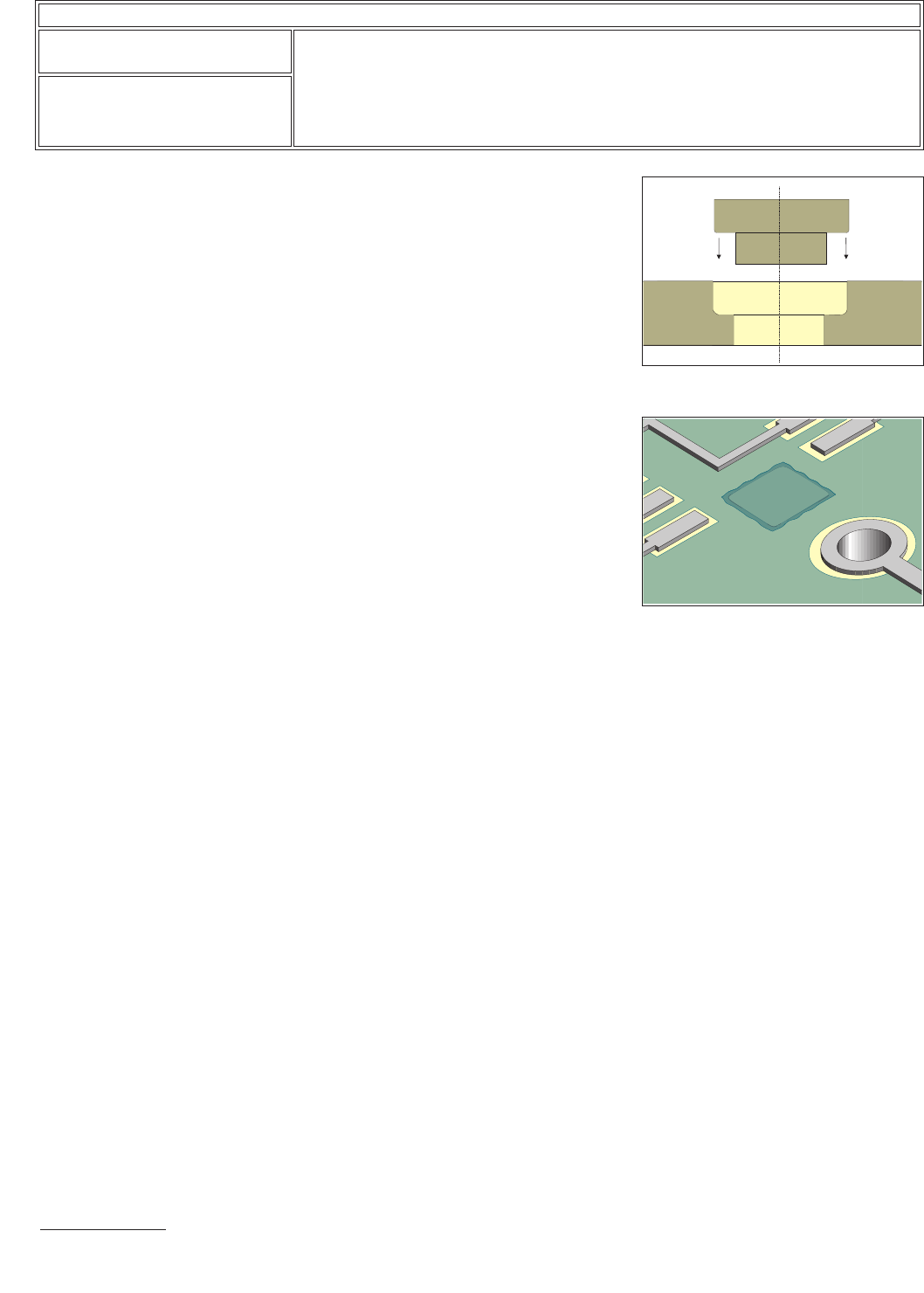
Figure 5 Bond replacement piece in
place.
Figure 6 Completed repair.
IPC-7721A
Number: 3.5.2
Revision:
Date: 2/98
Subject: Base Material Repair, Area Transplant Method
Page2of2
Copyright Association Connecting Electronics Industries
Provided by IHS under license with IPC
Not for Resale
No reproduction or networking permitted without license from IHS
--``,``,-`-`,,`,,`,`,,`---
OUTLINE
This procedure is used to repair mechanical or thermal damage to printed wiring
board base material. This method is used when extended areas of base material
must be completely replaced. This method may be used on single sided, double
sided or multilayer printed wiring boards or assemblies.
CAUTION
Surface conductors may need to be replaced in the damaged area. Be sure that the
appropriate conductor diagrams, or photographs reflecting the original conductors
are available so that they may be replaced after repairing the base board material.
Damage to internal conductors or planes may have to be restored using surface
wires.
REFERENCES
2.1 Handling Electronic Assemblies
2.2 Cleaning
2.5 Baking and Preheating
2.6 Epoxy Mixing and Handling
TOOLS & MATERIALS
Ball Mills, Carbide
Base Board Material
Carbide Saw
Cleaner
Cleaning Wipes
Color Agent, Various Colors
End Mills, Carbide
Epoxy
Hand Held Drill
Heat Lamp
Polyimide Tape
Knife
Oven
Precision Drill Press
Razor Saw
Scraper
PROCEDURE
1. Clean the area
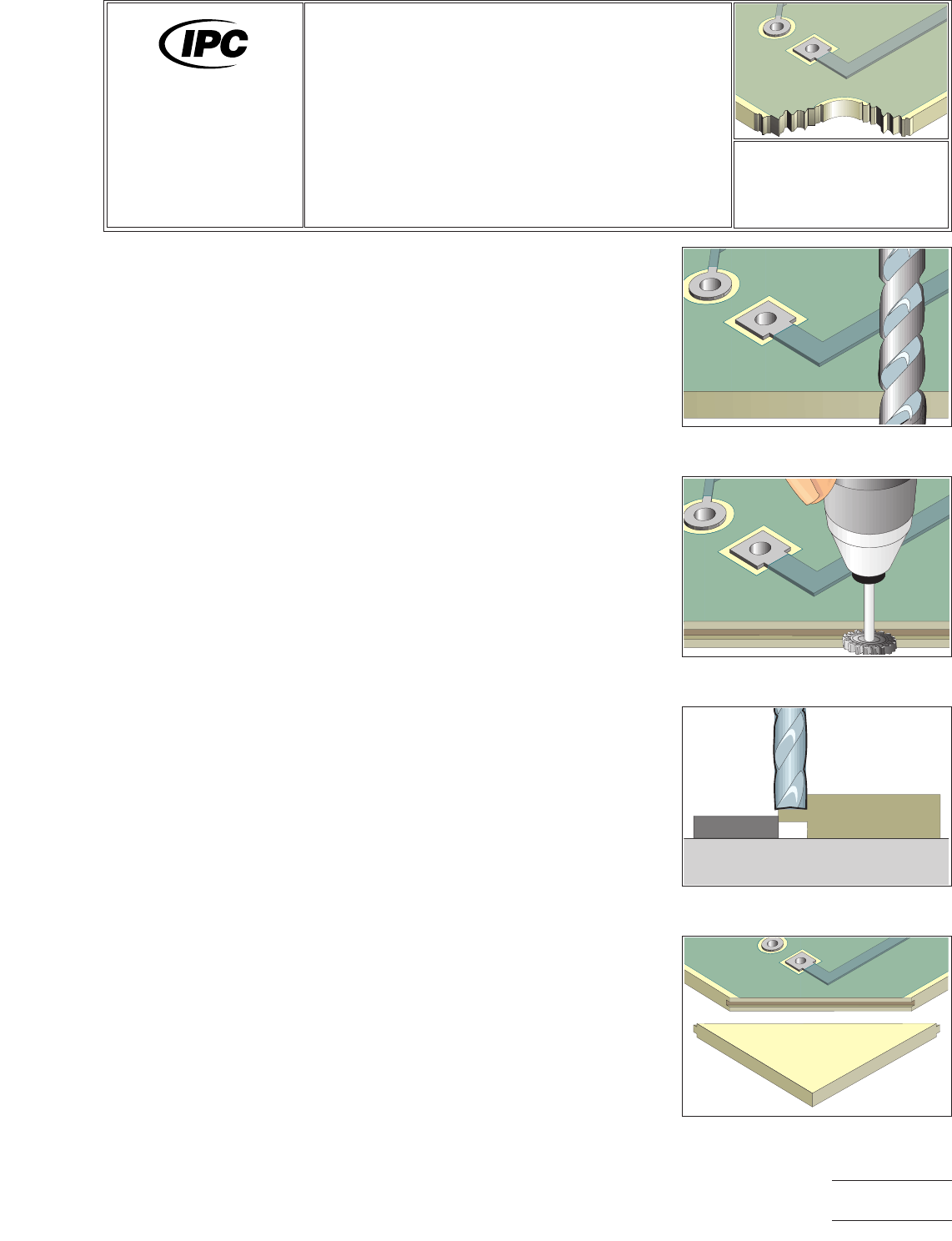
2. Cut away the damaged board material using a razor saw or milling cutter.
Remove all evidence of the damaged material. No fibers of laminate material
should be exposed. File the edge to ensure that the edge is flat. (See Figure 1.)
CAUTION
Abrasion operations can generate electrostatic charges.
CAUTION
Exercise care to avoid damage to any internal conductors. If any internal con-
ductors are damaged, surface wires may be required to restore electrical con-
nection.
3. Clean the area.
Figure 1 Cut away damaged base
material.
Figure 2 Cut a groove into the edge
of the PC board.
Figure 3 Mill a tongue onto the edge
of the replacement base material.
Figure 4 Check fit of new base
material.
7721A
Repair and
Modification of
Printed Boards and
Electronic Assemblies
Revision:
Date: 2/98
Base Material Repair,
Edge Transplant
Method
Number: 3.5.3
Product Class: R, W
Skill Level: Expert
Level of Conformance: High
Material in this manual was voluntarily established by Technical Committees of IPC. This material is advisory only and its use
or adaptation is entirely voluntary. IPC disclaims all liability of any kind as to the use, application, or adaptation of this material.
Users are also wholly responsible for protecting themselves against all claims or liabilities for patent infringement. Equipment
referenced is for the convenience of the user and does not imply endorsement by IPC.
Page1of2
Copyright Association Connecting Electronics Industries
Provided by IHS under license with IPC
Not for Resale
No reproduction or networking permitted without license from IHS
--``,``,-`-`,,`,,`,`,,`---
4. Install a carbide saw into the hand held drill. Set the speed to maximum and
machine a groove in the edge of the printed wiring board where the new base
material will be installed. The groove must be centered in the edge to ensure
that the new piece will fit properly. The groove width should be approximately
1/3 of the printed wiring board thickness. The groove depth should be approxi-
mately double the groove width. (See Figure 2.)
5. Cut a piece of replacement base board material that is the same thickness and
type as the piece removed. The replacement piece may be oversized, the
excess material will be removed after the replacement piece has been epoxied
in place.
6. Install an end mill into the chuck of a precision drill press. Machine a tongue
onto the entire mating edge of the replacement base material. The dimensions
of the tongue should match the size of the milled groove. (See Figure 3.)
7. Where required apply Polyimide tape to protect exposed parts of printed wiring
board bordering the prepared area.
8. Check the fit to be sure the new base material properly mates with the groove
in the printed wiring board. (See Figure 4.)
9. Mix the epoxy.
10. Coat both the tongue and groove surfaces with epoxy and fit together. Remove
excess epoxy.
11. Cure the epoxy per the manufacturers instructions.
CAUTION
Some components may be sensitive to high temperature.
12. After the epoxy has cured remove the Polyimide tape.
13. If needed, scrape off any excess epoxy using a scraper or knife.
NOTE
If needed, apply additional thin coating to seal any scrapped areas.
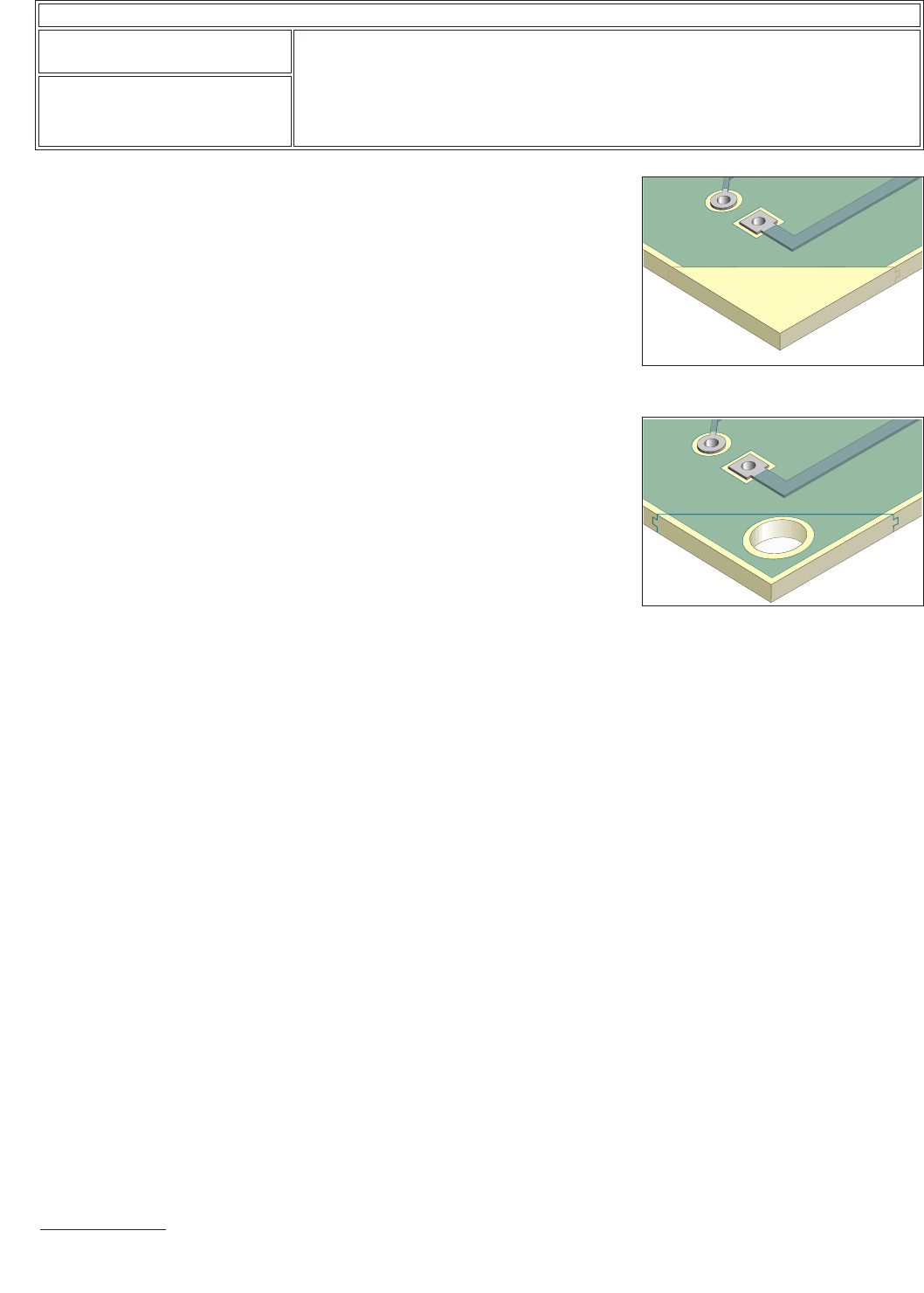
14. Saw or mill off excess base material and file flush with existing edge. (See Fig-
ure 5.)
15. Clean the area.
16. Complete by drilling holes, slots, etc. or adding circuitry as required. (See Figure
6.)
17. If needed, replace solder resist or conformal coating.
EVALUATION
1. Dimensions of area replaced should be checked to conform to specifications
required.
NOTES
Figure 5 Saw off excess new base
material.
Figure 6 Complete by drilling holes,
or adding circuitry as required.
IPC-7721A
Number: 3.5.3
Revision:
Date: 2/98
Subject: Base Material Repair, Edge Transplant Method
Page2of2
Copyright Association Connecting Electronics Industries
Provided by IHS under license with IPC
Not for Resale
No reproduction or networking permitted without license from IHS
--``,``,-`-`,,`,,`,`,,`---