IPC 7711A.pdf - 第322页
5. Inspect the proposed path for the foil jumper to ensure proper clearance. Use a milling machine to mill a shallow groove in the solder mask surface from the BGA pad area to the perimeter of the BGA site. Tight spacing…
OUTLINE
This method is used to change a circuit path at a BGA site for engineering changes
or modifications.
NOTE
This procedure requires precision milling equipment and highly trained technicians.
CAUTION
This procedure is not applicable for ‘‘via in pad’’ applications.
REFERENCES
1.0 Foreword
2.1 Handling Electronic Assemblies
2.2 Cleaning
2.5 Baking And Preheating
2.6 Epoxy Mixing and Handling
4.2.1 Conductor Repair, Foil Jumper, Epoxy Method
4.4.3 Surface Mount, BGA Pad Repair, Film Adhesive Method
6.1 Jumper Wires
TOOLS & MATERIALS
BGA Rework System
Bonding Iron
Bonding Tips
Bonding System
Buffer
Circuit Frames, BGA Pads
Cleaner
Drill System
End Mills
Epoxy
Flux, Liquid
Foil Jumpers
Heat Lamp
Microscope
Milling System
Oven
Precision Knife
Repair System or Repair Kit
Scraper
Solder
Soldering Iron
Tape, High Temperature
Tweezers
Wipes
PROCEDURE
1. Clean the area.
2. Remove the BGA component if installed, remove excess solder from the pads,
and clean and inspect the site using standard BGA rework equipment.
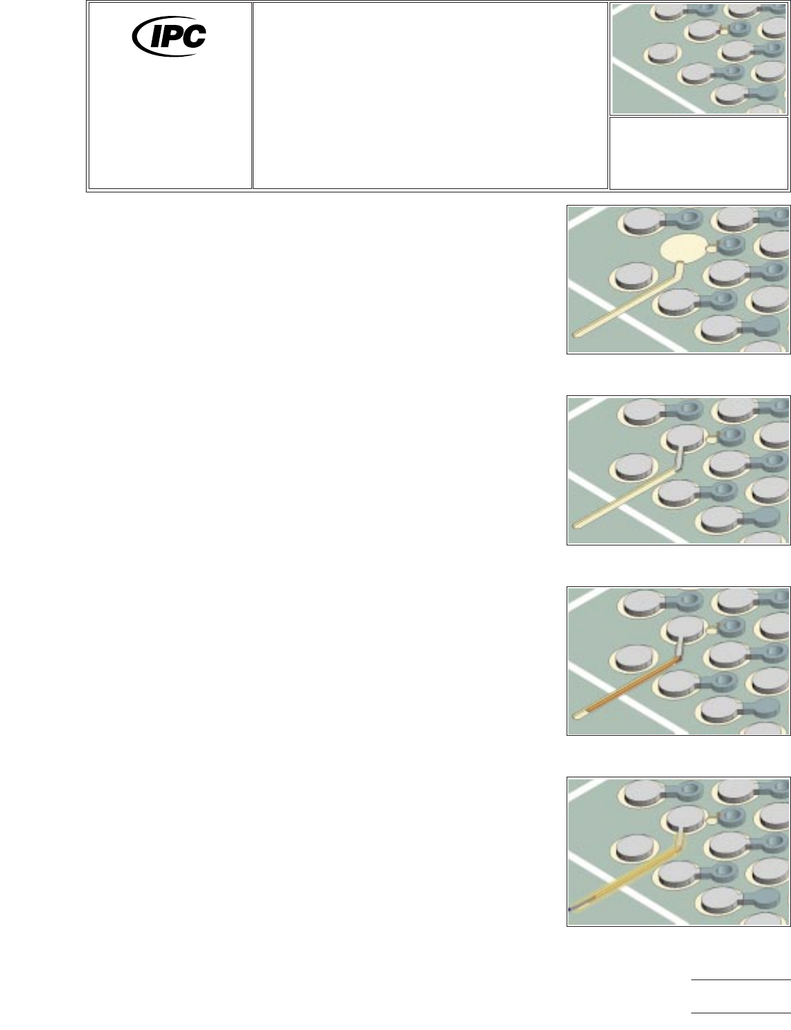
3. Cut the short conductor (dog bone) connecting the BGA pad to the connecting
via using a drill system or milling machine and appropriate size end mill. (See Fig-
ure 1 and 6.)
4. Remove the existing BGA pad. Apply heat from a soldering iron if needed. (See
Figure 2.)
Figure 1 Cut the connection to the via
using a drill system.
Figure 2 Remove BGA pad & mill shal-
low channel into solder mask surface.
Figure 3 Bond a new BGA pad in
place.
Figure 4 Solder a foil jumper to the
tail extending from the new BGA pad.
7721A
Repair and
Modification of
Printed Boards and
Electronic Assemblies
Revision:
Date: 11/99
Jumper Wires, BGA
Components, Foil
Jumper Method
Number: 6.2.1
Product Class: R/F
Skill Level: Expert
Level of Conformance: Medium
Material in this manual was voluntarily established by Technical Committees of IPC. This material is advisory only and its use
or adaptation is entirely voluntary. IPC disclaims all liability of any kind as to the use, application, or adaptation of this material.
Users are also wholly responsible for protecting themselves against all claims or liabilities for patent infringement. Equipment
referenced is for the convenience of the user and does not imply endorsement by IPC.
Page1of2
Copyright Association Connecting Electronics Industries
Provided by IHS under license with IPC
Not for Resale
No reproduction or networking permitted without license from IHS
--``,``,-`-`,,`,,`,`,,`---
5. Inspect the proposed path for the foil jumper to ensure proper clearance. Use a
milling machine to mill a shallow groove in the solder mask surface from the
BGA pad area to the perimeter of the BGA site. Tight spacing may restrict the
width of the channel to 0.25 mm [0.010 in] or less. Use a carbide end mill
approximately 0.050 mm [0.002 in] wider than the new connecting circuit. (See
Figure 3.)
NOTE
Be sure to mill a shallow groove to prevent damage to internal conductive lay-
ers.
6. Bond a replacement BGA pad in place using a bonding system. (See Procedure
4.7.3.) The new BGA pad must have a tail that will align with the foil jumper to
be added next. (See Figure 4.)
7. Select a foil jumper to match the width and thickness of the circuit to be
replaced. Cut a length approximately as needed. The foil jumper should overlap
the BGA tail section a minimum of two times the circuit width.
8. Gently abrade the top and bottom ends of the new foil jumper with the buffer to
remove any oxidation and clean.
NOTE
If needed, the ends of the foil jumper may be tinned with solder prior to lap sol-
dering in place.
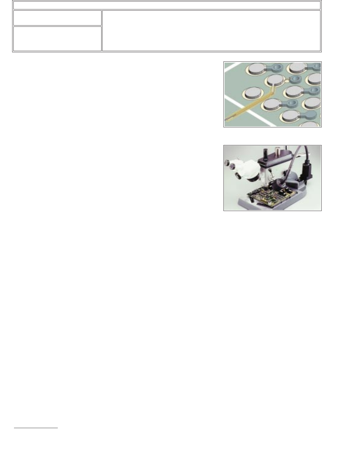
9. Position this new foil jumper along the milled groove. The foil jumper should
overlap the existing circuit a minimum of two times the circuit width. (See Figure
4.)
10. Apply a small amount of liquid flux to the overlap joint.
11. Lap solder the foil jumper to the BGA tail section using solder and a soldering
iron. Make sure the foil jumper is properly aligned.
12. Clean the area.
13. Mix epoxy. If desired, add color agent to the mixed epoxy to match the printed
wiring board color.
14. Coat the top and bottom of the foil jumper with epoxy. The epoxy bonds the
new circuit to the base board material and insulates the circuit. (See Figure 5.)
CAUTION
Some components may be sensitive to high temperature.
16. Clean the board as required.
17. Install new BGA per applicable procedures.
18. Solder one end of a fine gauge wire to the end of the extending foil jumper. (The
opposite end of the wire will be soldered later.) (See Figure 5.)
19. Route and terminate the other end of the jumper wire.
EVALUATION
1. Visual examination for alignment and overlap of new circuit.
2. Visual examination of epoxy coating for texture and color match.
3. Electrical tests as applicable.
Figure 5 Solder a wire to the foil
jumper bond with epoxy.
Figure 6 Sample of drill system used
to cut the connection from the BGA
pad to the via.
IPC-7721A
Number: 6.2.1
Revision:
Date: 11/99
Subject: Jumper Wires, BGA Components, Foil Jumper Method
Page2of2
Copyright Association Connecting Electronics Industries
Provided by IHS under license with IPC
Not for Resale
No reproduction or networking permitted without license from IHS
--``,``,-`-`,,`,,`,`,,`---
OUTLINE
This method is used to add a foil jumper at a BGA site by running the foil jumper
through a hole in the board. This method is normally used for engineering changes
or modifications.
NOTE
This procedure requires precision milling equipment and highly trained technicians.
This method is used when there is a buried via, and other methods of terminating to
the opposite side are not an option.
REFERENCES
1.0 Foreword
2.1 Handling Electronic Assemblies
2.2 Cleaning
2.5 Baking and Preheating
2.7 Epoxy Mixing and Handling
6.1 Jumper Wires
TOOLS & MATERIALS
BGA Rework System
Buffer
Cleaner
End Mills
Epoxy
Flux, Liquid Foil Jumper
Heat Lamp Microscope
Milling System
Oven
Precision Drill System
Precision Knife
Scraper
Solder
Soldering Iron
Tape, High Temperature
Teflon Sleeving
Tweezers
Wipes
Wire
PROCEDURE
1. Clean the area.
2. Remove the BGA component if installed, remove excess solder from the pads.
Clean and inspect the site.
3. Remove solder mask from the via pad terminating to the subject BGA pad.
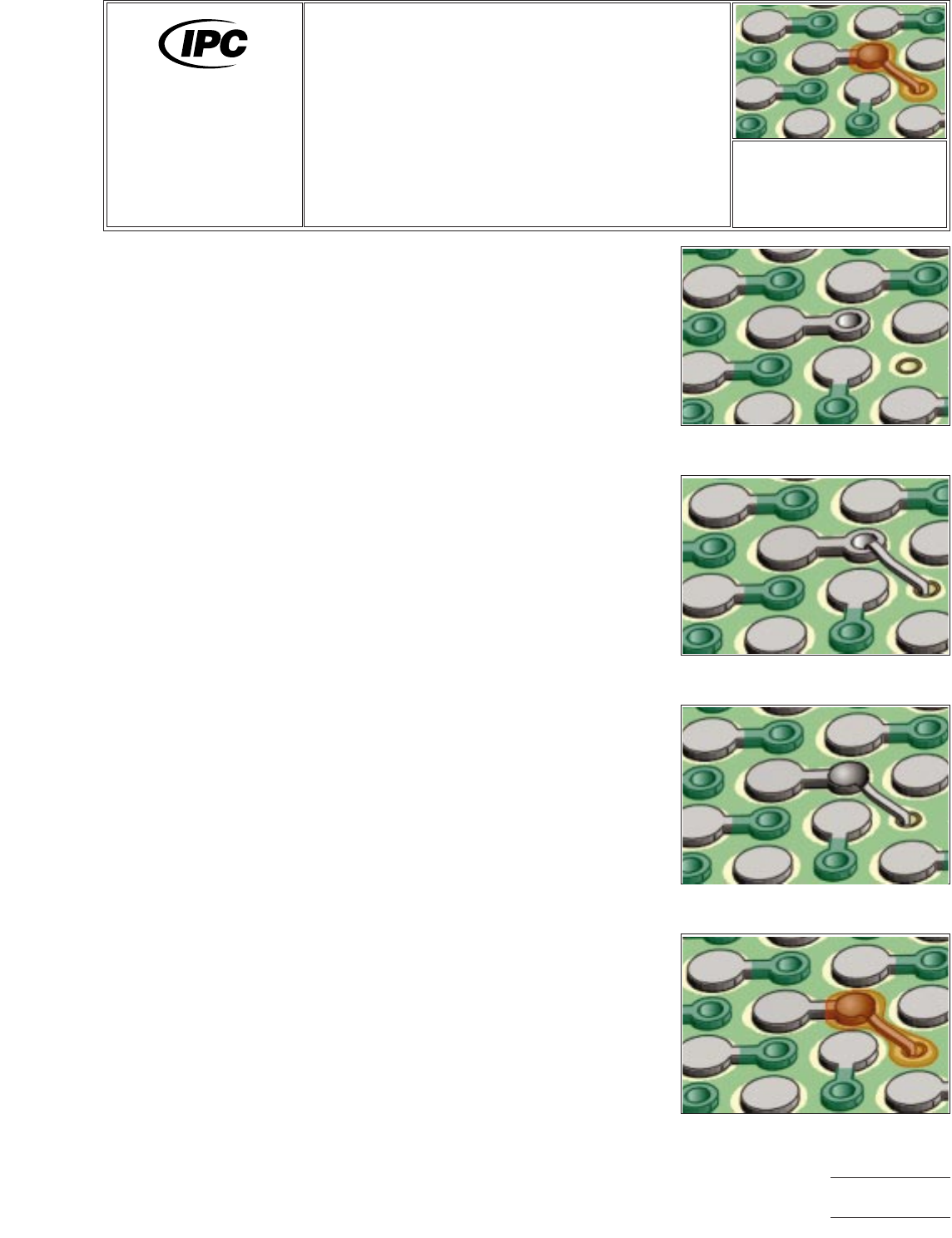
4. Mill a hole through the board at the precise coordinates using a Precision Drill
System and End Mill of the appropriate size. (See Figure 1 and 5.)
NOTE
Although both power and ground planes may be cut, inner layer signal traces
must be avoided.
5. Carefully inspect the milled hole and clean the area.
Figure 1 Mill a hole through the board
and insert a Teflon sleeve.
Figure 2 Insert a copper foil jumper
into the plated hole and Teflon sleeve.
Figure 3 Solder the foil jumper to the
plated hole connected to the BGA pad.
Figure 4 Overcoat the new connection
with epoxy.
7721A
Repair and
Modification of
Printed Boards and
Electronic Assemblies
Revision:
Date: 10/03
Jumper Wires, BGA
Components, Through
Board Method
Number: 6.2.2
Product Class: R/F
Skill Level: Expert
Level of Conformance: High
Material in this manual was voluntarily established by Technical Committees of IPC. This material is advisory only and its use
or adaptation is entirely voluntary. IPC disclaims all liability of any kind as to the use, application, or adaptation of this material.
Users are also wholly responsible for protecting themselves against all claims or liabilities for patent infringement. Equipment
referenced is for the convenience of the user and does not imply endorsement by IPC.
Page1of4
Copyright Association Connecting Electronics Industries
Provided by IHS under license with IPC
Not for Resale
No reproduction or networking permitted without license from IHS
--``,``,-`-`,,`,,`,`,,`---